Hot Filament Chemical Vapor Deposition of Crystalline Boron Films
Article information

Abstract
This article reports on the conditions required for the growth of crystalline boron films on silicon substrates by hot filament chemical vapor deposition method. The reactive gas was 3% diborane diluted in hydrogen. The films were characterized by optical, electronic, and atomic force microscopies; x-ray diffraction; and energy dispersive, electron energy loss, Raman, x-ray photoelectron, and Auger spectroscopies. The parameters that affect the morphologies of the films have been investigated. It was concluded that faceted crystals are produced at low B2H6 flows and working pressures below 200 mT. α-boron is produced between 530 and 600°C. Deposition outside this range produces thin films with a wide variety of morphologies. This result indicates that the films crystallize through a process called “abnormal or discontinuous grain growth.” It is assumed that this is due to the anisotropic surfaces of boron allotropes.
1. Introduction
Boron and boron compounds are remarkable materials with excellent physical properties such as high hardness, low densities, high melting temperatures, and distinctive thermal and electric transport properties.1,2) A remarkable example is MgB2, as it shows the highest critical temperature amongst conventional superconductors: 39 K.3) Crystalline boron is the second hardest elemental substance after diamond owing to the inherent stability of the B-B bonds.4) A potential application of boron films is as protective coatings, since they exhibit high hardness and low brittleness; in addition, the boron surface is oxidized when exposed to ambient air, producing a hydroxide layer that can act as a solid lubricant.5) Despite this, thin films of pure boron have seldom been used as high hardness coatings owing to the technological difficulties in producing homogeneous and crystalline films.6) Boron is a difficult material to work with because of the variety of systems in which it crystallizes and the diversity of morphologies that can be obtained with it. The phase diagram of elemental boron is still controversial, and it is possible that some of its allotropes have not yet been discovered.7) Boron exhibits four main allotropes that are arranged in a framework of icosahedral motifs (B12):8) β-rhombohedral, where the B12 motifs are present on the edges of the cell; α-rhombohedral, where the B12 icosahedra are positioned at the vertices of the rhombohedral unit cell; γ-orthorhombic phase, with a rock-salt type arrangement; and the amorphous phase, in which the long-range order is lost, but the short-range order of the B12 icosahedra is retained.5) Single crystals of α-boron can be prepared from a boron-platinum melt at high pressures (6–11 Pa) and temperatures.9) Boron films have been prepared by several methods, including plasma-assisted CVD of boron trichloride10,11) and diborane;12) laser ablation;5) magnetron sputtering;13) pyrolysis;12) and thermionic vacuum arc.12) Since boron films are excellent candidates for the development of novel devices1–3,5,14,15) we think it is convenient to study their growth by means of hot filament chemical vapor deposition (HFCVD) method. HFCVD is an established coating method for diamond films. For a more detailed description of the method, we suggest to the readers our previous work, where the reactor has been completely characterized by computational models that were resolved numerically;16) this is the same reactor that was utilized in the present work. The HFCVD method has been scaled to coat large area surfaces17) with good homogeneity, 18) in addition, processes for Diamond Like Carbon (DLC) coating of three-dimensional base shapes are obtainable.19) The hypothesis is that if this technique is suitable for depositing diamond films, there is also a window of conditions in which crystalline boron films can be produced.20) Consequently, much of the development that has been carried out to obtain DLC films could be transferred to the production of boron films. For this work, we used as the initial parameters the conditions that were successful for the production of the best diamond crystals (i.e., CH4 diluted in hydrogen), knowing in advance that these conditions may differ for the case of boron films. The parameters were determined by trial and error, but, once the optimal conditions were found, they were used multiple times to ensure the reliability of the experiments. The films were characterized by various techniques, including optical, electronic, and atomic force microscopies, x-ray diffraction (XRD), and energy dispersive (EDS), electron energy loss (EELS), Raman, x-ray photoelectron (XPS), and Auger spectroscopies.
2. Experimental Procedure
2.1. Experimental
The thin films investigated in this study were grown by using a HFCVD setup.16) The reactor chamber consisted of a 50.8 mm diameter quartz tube evacuated with a vane pump. A 10 ml min−1 mass flow controller was employed to supply a pre-mixture of 3% B2H6 in H2. Since diborane is a very toxic substance, it is recommended to obey the safety precautions when handling it. The filaments were fabricated with seven loops of 99.5% tungsten wire with the diameter of 0.65 mm. A small volume thermal shield was provided that isolated the region between the filament and the substrate holder from the rest of the chamber. The heat-shield was made of stainless steel. The shield is important to achieve uniformity of films, as it homogenizes the heat dissipated by the filament. The temperature of the substrate was measured by a type-K thermocouple attached to the back side of the substrate. The filament current was provided by a 30 A power supply regulated in constant-current mode. The temperature of the filament was established as 1900°C by an optical pyrometer at the beginning of the depositions. The separation between the filament and the substrate in all the runs was fixed to 4 mm, and the filament was placed 10 mm away from the gas inlet; heating of the substrates was achieved by the filament radiation.
Boron films were deposited on silicon wafer substrates with orientation (100) or (111). To improve the nucleation, the substrates were abraded with 1 μm diamond paste, followed by 5 min ultrasonic cleaning in acetone. The system base pressure was 40 mT and the working pressure around 190 mT. For the sample reported here, the filament current, If, was fixed at 25.5 A, and the B2H6 flow rate set to 4 ml min−1. Since the resistance of the filament fluctuates as it reacts with boron, the filament voltage, Vf, also changes. The starting Vf for a new filament was around 14 V; it then increased up to 16 V, before decreasing and stabilizing at 13.5 V. Following the changes in the input power, the substrate temperature was slowly varied from 530 to 600°C and then stabilized at 575°C. Some deposits were obtained outside this range of conditions to show the large number of morphologies that can be obtained by depositing boron by the HFCVD method.
Film analyses were carried out by using several techniques. Scanning electron microscopy (SEM; JEOL JSM-5300) was coupled with energy-dispersive spectroscopy (EDS) by using an X-ray detector for analysis. Atomic force microscopy (AFM; Park System model XE-70), XRD (Panalytical X’pert Pro MRD), Raman spectroscopy (Lambda Solutions Dimension P2 instrument) in back-scattering geometry with a laser wavelength of 531.5 nm @ 5 mW, resolution of 3 cm−1, and spot size of 5 μm, X-ray photoelectron spectroscopy (XPS), Auger spectroscopy, and electron energy loss spectroscopy (EELS; carried out on a Specs instrument) were performed. For XPS, the instrument was operated with monochromatic Al Kα irradiation (photon energy 1476.6 eV and pass energy 29.4 eV). For EELS, the primary electron energy was set to 1000 eV. For Auger spectroscopy, the primary energy was 3000 eV. The samples for transmission electron microscopy (TEM) were obtained by sonicating the substrate film in acetone to detach some grains from the film; then, the solution was directly dropped on 400 mesh copper grids coated with carbon films. Excess acetone was allowed to evaporate in air. The TEM grids were examined in a JEOL JEM-2010 microscope operated at 200 kV.
3. Results
The richness of the morphologies and structures of boron films is wide, as mentioned in the introduction section; therefore, in this work, we will emphasize the films that showed faceted crystals similar to those revealed by the DLC films. Other morphologies will be presented as evidence of the possibility of producing other types of materials from boron; some of them are shown in the supplementary material without further discussion.21) The faceted boron thin films were deposited according to the parameters indicated in the experimental section. Abrasion of the substrate with diamond paste is very important, because, if the films are deposited without performing this step, the type of crystal obtained can vary greatly. Their morphological characteristics were observed by using optical and electron microscopes (Fig. 1), and atomic force microscope (Fig. 2). The deposition time for the film presented was 4 h, and substrate temperature around 575°C. As is possible to appreciate from the micrographs, the surface is covered with faceted grains of varying sizes between 3 and 15 μm. The grains are joined together to form a continuous film. A circular substrate area of ~ 100 mm2 is covered with grains of similar characteristics, which is remarkable considering that the HFCVD technique often produces uneven films. Beyond this area, the shape of the crystals changes gradually, as shown in the supplementary data.21) The experimental conditions are similar to those used to deposit diamond films by the HFCVD method in references 14 and 15, except that the CH4 gas is replaced by B2H6. It is important to keep in mind that, unlike DLC deposition, the parameter window is narrow. For relatively small changes in the conditions, materials with different morphological characteristics are produced, like filaments, cone-shaped crystals, whiskers, foils, and flower-like materials; some of them are shown in supplementary data.21) As a consequence, if we try to change the crystal sizes by adjusting the B2H6 flow, as can be achieved in the case of DLC films grown under CH4 flow, then, the morphological characteristics change radically. Because of this, many tests were conducted to confirm the set of experimental parameters. It was concluded that the faceted crystals are produced at B2H6 flow rates of 3–5 ml min−1, working pressures below 200 mT, and substrate temperatures higher than 530°C and lower than 600°C. The only parameter that we found useful for regulating the crystallite size was deposition time, when all the other parameters were kept constant.
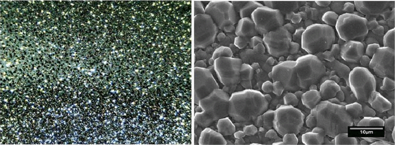
Morphology of boron films obtained by optical microscopy in an area of 1.2×1.5 mm, and an enlarged SEM image. Faceted crystals of variable sizes are observed to be distributed uniformly on the surface.
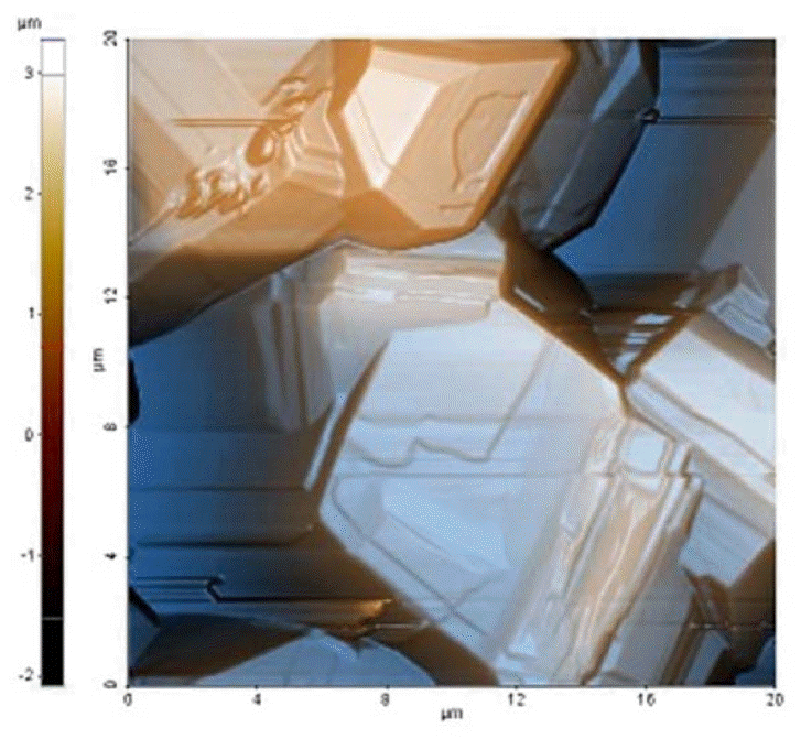
Atomic force scanning image of the boron crystals. It shows in detail the roughness and the faceted structure of the grown crystals.
To determine the film composition, several spectroscopic investigations were carried out. By EDS, the elements detected were silicon and oxygen from the substrate, since our spectrometer is blind to boron. The tungsten signal was missing in the EDS pattern, which indicated that the films were free from contamination of the filament material; then, we ruled out the formation of boron-rich tungsten compounds. Fig. 3 shows the Auger spectrum in differentiated mode after sputtering with Ar+. The elements identified by Auger spectroscopy are boron, carbon, and argon; the argon LMM signal comes from the Ar+ implanted within the film. No oxygen was detected by AES, except before the sputtering. The film composition according to AES was 88% B and 12% C (atomic percent). The B-KLL shape is similar to the C-KLL shape reported for diamond, with two shoulder peaks corresponding to the low-energy side of the main transition.22) The fine structure of Auger spectroscopy was used to identify the hybridization of carbon in the DLC films.22,23) The fine structure results from energy losses that occur after the Auger ionization process. These losses might provide a fingerprint of the nature of bonding within the material. Fig. 4 shows the EELS pattern with the excitation energy of 1000 eV. Two losses are clearly discernible, one as a shoulder of the backscattered electron with an energy around 4 eV, and the second with an energy of 24 eV. It should be noted that the fingerprint of EELS is similar to the characteristic losses of graphite. In graphite, the relative weak peak observed near 4 eV is attributed to a hybrid resonance from the cooperative behavior of π electrons screened by σ-electrons.24) This loss is absent in sp3-hybridized DLC, and it is considered to be the evidence of a π-system, which is related to sp2 hybridization, like the carbon in graphite. It indicates the presence of pz orbital, which can be viewed as an external orbital to the in-plane bonds. A similar interpretation can also be applied to boron compounds. A boron compound displays two kinds of bonds related to B12 motif: intra-bonds and extra-bonds. The number of intra-icosahedral bonds is much higher than the number of inter-icosahedral bonds. We assume that the 4 eV losses result from the collective behavior of the extra-icosahedral bonds. The 24 eV loss can be considered as a collaborative resonance involving the participation of the intra- and extra-bonds; then, the peak position depends on the total number of electrons of boron. Consequently, the main peak is directly related to the specimen density. The free-electron approximation (equation 1 below) can be applied to determine the electronic density (ρe) by using the peak position, Ep, from the EELS measurements. The mass density (ρm) can be calculated from the electronic density (equation 2):
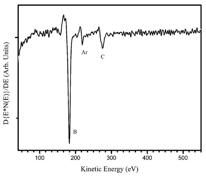
Auger spectrum of a boron film grown by HFCVD. The fine structure of B-KLL is similar to that of diamond.
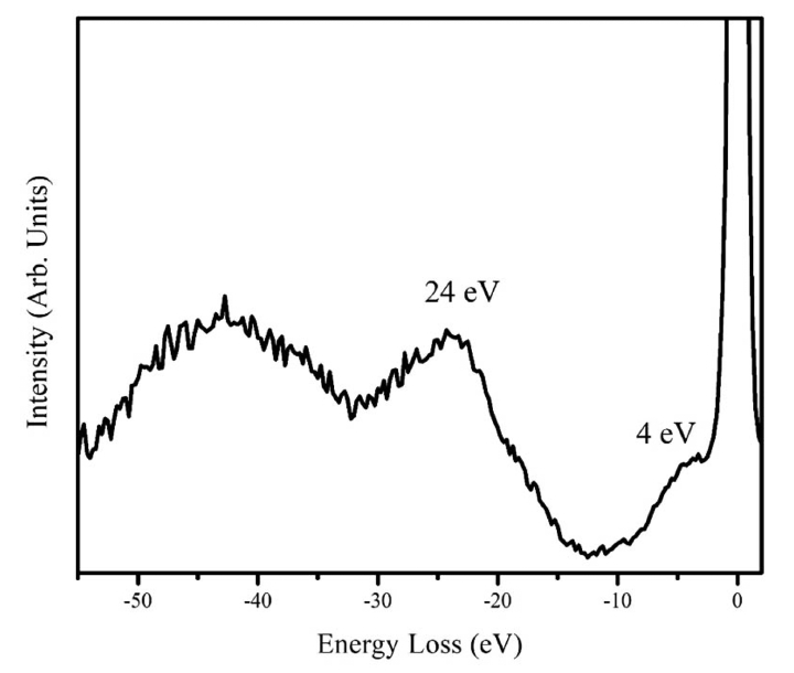
Electron energy loss spectrum of a boron film grown by HFCVD. The peak near 4 eV is from π-electrons, and the peak at 24 eV is due to the σ-electrons.
where me is the electron mass, e is the electron charge, ɛ0 is the permittivity of free space, NA is the Avogadro number, and is Planck’s constant divided by 2π; CB and MB are the number of electrons and the mass of boron atoms, respectively. According to the above expressions, the electronic density of our film is 4.1×1023 cm−3, and the mass density 2.49 g cm−3. The mass densities of the different allotropes of boron are reported as 2.46 [α-rhombohedral boron]; 2.29–2.39 [α-tetragonal]; 2.35 [β-rhombohedral]; 2.36 [β-tetrahedral]; and 2.52 g cm−3 [orthorhombic]. EELS analysis points to a high density of the boron film, however, the EELS peaks are wide and not clearly defined, therefore, the determinations of the densities are not infallible. However, this analysis indicates that the EELS pattern originates from a high-density boron film.
Figure 5 shows the high-resolution XPS energy regions for boron, carbon, and oxygen. The intensities for the carbon and oxygen graphs are multiplied by a factor of three. By means of semi-quantitative XPS analysis by using standard sensitivity factors, the atomic concentrations are obtained as 77% boron, 16% carbon, and 7% oxygen. The chemical contributions were revealed by fitting Gaussian-Lorentzian functions to the peak profiles. In the O 1s region, a single peak was observed centered at 533.0 eV, which matched with the binding energy of B2O3.25) As the O 1s intensity accounts for only 7%, we assume that oxygen atoms are present only on the surface of the film as a B2O3 overlayer, which is in concurrence with the results of Auger spectroscopy, which revealed no oxygen in the bulk. The B 1s spectrum has three contributions. The peak to the high energy side, at 191.3 eV, can be assigned to the formation of bonds between boron and oxygen that shape the B2O3 overlayer.25) The peak to the low energy side, at 186.5 eV, is attributed to B-C bonds, similar to those observed in B4C.25) The principal contribution at 188.4 eV corresponds to the predominant B-B bonding of the film.25) In the C 1s energy window, two main Gaussian peaks are observed. The 282.7 eV peak is assigned to C-B bonds, whereas the peak at 285.1 eV corresponds to graphite-like species. The area ratio between the 285.1 and 282.7 eV peaks is 8.5. This suggests that only ~ 2% of the carbon atoms are bound with boron; the remaining carbon atoms form graphite species. Following semiquantitative XPS analysis, the material was found to contain 83% boron, 15% graphitic carbon, and 2% B4C.

High-resolution XP spectra of the boron films in the B-1s, C-1s, and O-1s energy windows. The open circles correspond to experimental data and the colored lines to fitted components.
Figure 6 shows the XRD pattern of a film in Bragg-Brentano geometry. The experimental patterns were compared with the Inorganic Crystal Structure Database (ICSD), and we found the ICSD 61-2521 file to be the best match. According to this, the material should be tetragonal boron, with space group P42/nnm (134) and cell parameters a = 8.8000 Å and c = 5.0500 Å.26) All the experimental peaks could be indexed to the peaks included in this file; however, several expected diffractions were missing in the experimental pattern. The main peaks of the experimental pattern can also be indexed roughly to the ICSD file 181823 of α-boron,9) which is a trigonal crystalline system R-3m (166) with cell parameters a = 4.9065 Å and c = 12.5658 Å. From the XRD data, it was impossible to determine unambiguously the crystalline system because of the missing diffractions, which could be related to the texture of the film. It is interesting to note that although the film is composed of large crystallites, the count rate is very poor. The x-ray scattering cross section of boron is very low, and most of the film volume is occupied by empty spaces, as observed from the micrographs shown in Figs. 1 and 2; this explains the low counting ratios. In order to elucidate the crystalline system, Raman measurements were carried out. Fig. 7 shows a typical Raman spectrum of the boron film characterized in this study. For this spectrum, we picked a large crystal and focused a laser beam onto it. Three strong peaks are clearly discernible at 498, 878, and 1164 cm−1. They were compared with the literature data, and we found that the experimentally measured frequencies agree well with those reported in references 6–9 for α-rhombohedral boron. The vibrational modes corresponding to the wavenumbers 498 and 878 cm−1 are intra-icosahedral, and 1164 cm−1 can be classified as inter-icosahedral.9) Several vibrational modes of α-boron are missing in our spectrum,27) which can be related to changes in the short/long range order of the crystalline system.28) The TEM instrument is another excellent tool for determining the crystalline system. For example, in Fig. 8, a small crystal is shown that can be indexed to α-boron by using the TEM diffraction analysis program.29)
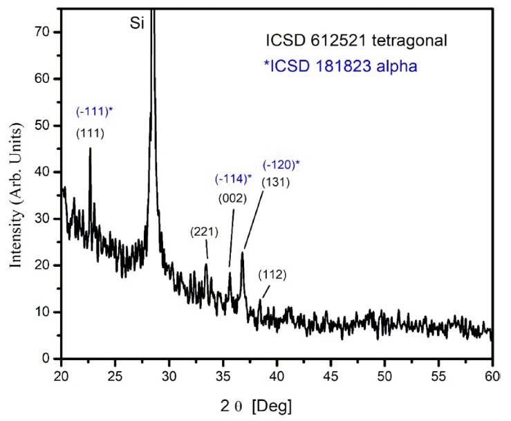
XRD pattern of a boron film grown by HFCVD that is indexed to ICSD files 612521 (tetragonal boron) and 612521 (α-boron).
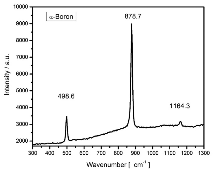
Raman spectrum of the boron crystal grown by HFCVD. The vibrational modes at 498 and 878 cm−1 are intra-icosahedral, and the 1164 cm−1 mode is inter-icosahedral.
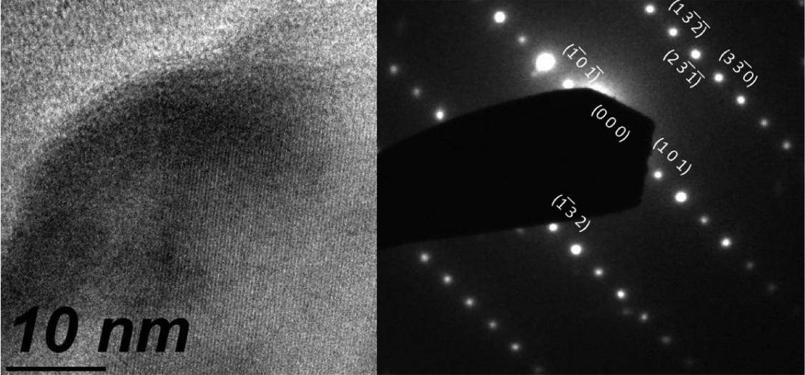
TEM image revealing the high crystallinity of the film, and the diffraction pattern of a selected area of a α-boron crystallite along the (111) zone axis.
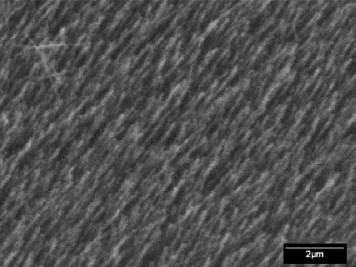
To study the kinetics of crystal growth, the deposition was interrupted after 10 min, keeping all the other parameters constant, and the films were analyzed by SEM. To induce nucleation, the silicon substrates were slightly abraded with diamond paste, and the scratches were either randomly distributed (Fig. 9) or in only one direction (Fig. 10). The initial stages of nucleation consist of small needleshaped crystals that are randomly distributed on the surface of the substrate, without a definite orientation, as shown in Fig. 9. On the contrary, Fig. 10 shows that needlelike crystals grow from a densified matrix along the abrasion lines in the substrate. Needles or fibers can also be produced from diborane by using the HFCVD method if the deposition conditions are outside the abovementioned range. As an example, in Fig. 11, the SEM image of the film produced at the substrate temperature of 700°C, B2H6 flow rate of 20 ml min−1, and P = 650 mTorr is shown. It reveals rounded particles and fibers that are several microns in length and having a thickness of approximately 1 μm. More fibrillary morphologies can be found in supplementary data.21)
SEM image showing early nucleation of boron films, with the substrate slightly abraded without a preferential direction by using a 1 mm diamond paste. Deposition time: 10 min, Ts = 530°C, and B2H6 flow rate: 4 ml min−1.
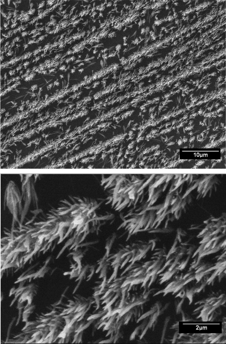
SEM images showing early nucleation of boron films, with the substrate slightly abraded in a single direction by using a 1 mm diamond paste. Deposition time: 10 min, Ts = 530°C, and B2H6 flow rate: 4 ml min−1.

SEM image of the fibrillary and rounded morphologies of a sample produced at Ts = 700°C, 650 mT pressure, and 20 ml min−1 B2H6 flow rate over an abraded substrate.
4. Discussion
The HFCVD method is based on chemical precipitation of films from a gas phase following activation of the reactive gas on hot filaments. Basically, it is a variant of the CVD method, where the activation energy is obtained from a hot filament. A CVD process is a non-equilibrium process and typically involves complex chemical reactions. The overall deposition rate of the CVD process may be limited by (i) the homogeneous reactions that take place in the gas phase, (ii) the heterogeneous reactions that occur on the surface of the substrate, and (iii) the mass-transfer of the precursors.28) CVD reactions with a high concentration of hydrogen help reduce oxide formation, as observed here, where oxide formation was low. One important advantage of HFCVD over other methods is its tendency to produce crystalline films. For example, Godet et al.30) prepared hydrogenated boron films by radio frequency plasma decomposition of diborane diluted in hydrogen in the temperature range 50–100°C; in contrast to our results, they reported the synthesis of amorphous films up to 950°C. Something important to keep in mind is that no author has reported on the formation of regular faceted crystals, which is the case with this work. Another difference is that metal seeds are not used here to promote nucleation, since the nuclei originates from the defects generated in the substrate by the abrasion of its surface.
As mentioned above, one of the main problems when working with boron is the diversity of morphologies that can be produced. This is evident from the results presented in this paper and the supplementary data,21) as well as those reported in the scientific literature. An interesting catalog of the richness of boron morphologies can be found in the work of Gao6) on crystals prepared from diborane diluted in hydrogen by using the vapor-liquid-solid method. From his work, Gao reported needles with lengths that ranged from several microns to about one hundred microns, and the diameter of the needles (near the base) was about 5 μm. Arguably, Gao determined from XRD patterns that the needles are actually silicon boride, but their elemental analysis did not show a significant amount of silicon. Similar behaviors have been reported by several researchers, an example being reference,31) where it was associated with boron nanowires. The experimental evidences indicate that boron can crystallize through a process called “abnormal or discontinuous grain growth.32)” Abnormal growth usually occurs during the formation of polycrystalline bodies where the seeds of crystals of different phases come into mutual contact through a common medium. In the course of thickening, some crystallites can grow more quickly at the expense of other grains, in violation of the uniform texture of the polycrystalline body.33) If the difference in the growth rates is very large between the phases involved, then the material can grow in 1D forms, such as nanorods or needles. As the results show, abnormal growth increases when the films are processed at higher temperatures and higher pressures, as observed in Fig. 11. The anomalous growth in boron seems to be very sensitive to variation in the growth parameters, as can be seen in the supplementary material, 21) where, in the same substrate, the shape of the crystals changes as a function of the distance to the center of the substrate. We believe that this is due to a gradient of the distribution of the reactive species,16) given the configuration of the reaction system. Similar morphologies were also reported by Gao.6) The abnormal growth of crystals is well documented for materials that exhibit polytypes, such as silicon carbide, CaTiO3, and SrTiO3 perovskites.33) It can be said that one of the main advantages of the HFCVD method of producing boron films is that it can keep abnormal growth under control in order to produce regular crystals.
5. Conclusions
The main objective of this research was to produce crystalline boron films by using the HFCVD technique that rival the DLC films produced through the same technique. This was achieved when uniform crystalline α-boron films were produced that were dispersed over a wide area of the substrate, and the conditions for their growth were determined. The main impurities were carbon and oxygen, which were located predominantly on the surface of the boron film. The crystalline system determined by using XRD is debatable, owing to the small cross-section of boron and the great similarity between the interplanar spacings of the different crystal systems. However, the set of evidences from TEM and Raman spectroscopy seems to indicate that it is a variety of α-boron, since the Raman lines agree well with the modes of vibration of this system. The experimental evidence also indicates that the boron films grow through a process called “abnormal or discontinuous grain growth.” Nevertheless, by using proper conditions, the discontinuous growth can be kept low to produce regular crystals. These results emphasize the need to continue research on the preparation of boron films by following the methodology used to grow diamond by CVD, as this strategy could save a lot of research effort.
Acknowledgments
The author would like to thank Francisco Ruiz, Jaime Mendoza, Jesús A. Díaz, Israel Gradilla, E. Murillo, D. Dominguez, and Eloisa Aparicio for their technical assistances.
Notes
Funding information: This work was supported by UNAM-DGAPA-PAPIME PE100318, PE101317, and UNAM-DGAPA-PAPIIT IA 101018, IN 112117, IN 110018, and IA 103117 projects, as well as by Conacyt through Fordecyt 272894 project.
Declarations of interest: none