Nonstoichiometric Effects in the Leakage Current and Electrical Properties of Bismuth Ferrite Ceramics
Article information
Abstract
To understand the defect chemistry of multiferroic BiFeO3-based systems, we synthesized nonstoichiometric Bi1+xFeO3±δ ceramics by conventional solid-state reaction method and studied their structural, dielectric and high-temperature charge transport properties. Incorporation of an excess amount of Bi2O3 lowered the Bi deficiency in BiFeO3. Polarization versus electric field (P-E) hysteresis loop and dielectric properties were found to be improved by the Bi2O3 addition. To better understand the defect effects on the multiferroic properties, the high temperature equilibrium electrical conductivity was measured under various oxygen partial pressures (pO2’s). The charge transport behavior was also examined through thermopower measurement. It was found that the oxygen vacancies contribute to high ionic conduction, showing pO2 independency, and the electronic carrier is electron (n-type) in air and Ar gas atmospheres.
1. Introduction
In February 2003, the Restriction of Hazardous Substances Directive (RoHS) was enacted in Europe and on July 1, 2006, a regulation was enacted restricting the use of lead, cadmium, mercury, hexavalent chrome, phthalates, and brominated flame retardants (PBBs, PBDEs) in electronic products and devices. After such enactments, the usage of lead was regulated, resulting in active research on lead-free (Pb-free) piezoelectric ceramics to replace PZT based materials. Representatively, studies on alkali metal based (Na0.5K0.5)NbO3 (NKN), bismuth based (Bi0.5Na0.5)TiO3 (BNT) and BiFeO3 (BFO) compositions are widely being carried out.1–4) BFO has a rhombohedral (R3c) structure and exhibits multiferroic properties, in which antiferromagnetic and ferroelectric properties coexist at room temperature.5) Also, BFO has significant advantages of a high Curie temperature (TC) of 827°C and high Neel temperature (TN) of 367°C.6) According to the literature, BFO shows a value of 90 – 100 μC/cm2 when the spontaneous polarization (PS) value is orientated in the [111] direction.7) Despite having such excellent properties, BFO is known to have limitations in applicability due to its high leakage current. The causes of the leakage current of BFO have been reported to be the combined effect of Bi volatility in the high temperature sintering process and defects of oxygen vacancies due to the transition metal Fe.8,9) Also, recent reports have shown the effects of secondary phases of BFO like Bi25FeO39 and Bi2Fe4O9, which appear in a specific temperature range (447 – 767°C).10,11) However, sufficient context is lacking to clearly explain the fundamental cause behind the leakage current due to the significant variation of material properties that result from Bi volatility and Fe transition. In this study, to measure the ferroelectric P-E hysteresis loop, dielectric constant, and dielectric loss at room temperature, and to investigate the leakage current mechanism of BFO, the amount of Bi vulnerable to high temperatures was controlled and nonstoichiometric BFO ceramics of Bi1+xFeO3±δ were fabricated. Additionally, so that the mechanism behind the main defects and charge transport, which cause the leakage current, could be understood, and in order to identify defects in a specific range, the electrical conductivity and Seebeck coefficient were measured at high temperature with various temperatures and oxygen partial pressures (pO2).
2. Experimental Procedures
In the case of BFO, it is known that fabricating a single phase is difficult due to the volatility and transition issues of the constituent elements. Single phase BFO can be synthesized when the constituent elements Bi2O3 and Fe2O3 have a stoichiometric ratio of exactly 1 : 1. However, since long-term exposure to high temperature is necessary for the ceramic sintering in the fabrication process, it is difficult to evade the temperature range (447 – 767°C) for secondary phase production. In order to overcome this issue, the powder produced after heat treatment was reacted with nitric acid to remove the secondary phase; sol-gel or hydrothermal methods were used to reduce the particle size; or spark plasma sintering (SPS) and rapid sintering were used to reduce the exposure time to the high sintering temperature.12,13) However, the above experiment involves cost and environmental issues because acids are used, like nitric acid for the fabrication. Thus, in this study, the general solid-state reaction method was used to prevent the production of the secondary phase after sintering; also, the quenching method was used to rapidly cool to room temperature for BFO ceramic fabrication.
2.1. Powder Synthesis and Specimen Preparation
Starting materials Bi2O3 (Alpha acer 99.99%) and Fe2O3 (Alpha acer 99.99%), of high purity, were used to fabricate BFO. The mol% values of the starting materials were calculated and weighted according to Bi1+xFeO3±δ (x = 0, 0.05). Then, ethanol was used as the solvent, along with the ZrO2 balls, to carry out ball milling for 24 h to improve the homogeneity of mixed powder. Afterwards, each specimen was denominated as 0BFO (x = 0) and 5BFO (x = 0.05). The mixed powder was dried using a dryer and the dried material was heat treated at 700°C under ambient air conditions for 2 h. After the heat treatment, the material was ground in a mortar to improve the powder homogeneity and PVA (polyvinylalcohol) was added to enhance the integration between the powders. The homogeneity of the PVA-added powder was further improved through sieving and the ceramic was fabricated using a uniaxial press.
2.2. Sintering Process
Microstructure observation of the BFO ceramic fabricated using the general sintering method (Fig. 1(a)), which performs sintering by raising the temperature to the final sintering temperature in one step, revealed nonuniform grains and voids here and there.14,15) Such voids were observable due to numerous variables including the sintering temperature, sintering time, and heating rate. The two-step sintering method was used to effectively improve such problems in the sintering process.16) In order to resolve the reaction issue during high temperature sintering between the Al2O3 and Bi ion of the BFO, a sufficient amount of BFO powder was applied on an alumina plate to prevent direct reaction between the BFO specimen and Al2O3. In addition, in order to prevent Bi ion volatility, which can occur during the high temperature sintering process, sintering was carried out after sufficient application of the BFO powder on the BFO specimen. Also, the temperature of 300°C was maintained for 1 h to remove the PVA in the specimen; then, the temperature was rapidly raised at a rate of 10°C/min to reduce defects that can occur in the secondary phase generation range of 447 – 767°C. Then, after maintaining a temperature of 750°C for 30 minutes, the heating rate was decreased to 2°C/min in order to reduce problems like voids within the ceramic; heating was continued until the final sintering temperature of 820°C. Finally, the temperature of 820°C was maintained for 10 minutes; this was followed by air quenching for rapid cooling until room temperature was reached, so that secondary phase generation during cooling can be prevented. Fig. 1(b) shows the overall two-step sintering process. The structure and crystallinity of the produced specimen were analyzed through XRD (X-ray Diffractometer, Miniflex II, Rigaku); SEM (Scanning Electron Microscope, SEM, JSM-6510) was carried out for microstructural observation.

Conditions for (a) conventional sintering and (b) two-step sintering process; air-quenched (AQ) and furnace-cooled (FC).
2.3. Electrical Conductivity Measurement
After cutting the Bi1+xFeO3±δ (x = 0, 0.05) specimen to dimensions of 2 × 2 × 15 mm3, sputtering was used to apply platinum electrodes at regular intervals on the specimen surface. Each of the 4 platinum electrodes was connected to platinum wires and the electrical conductivity was measured for the temperature range of 650 – 750°C. To eliminate the issue of non-ohmic contact, the electrical conductivity was measured using the 4-probe method. The following equation was used to convert the resistance obtained from the specimen measurement to the electrical conductivity.
Here, R is the resistance [Ω], A is the specimen cross-section area [cm2], and l is the distance between the electrodes [cm].
Ar (99.999%) gas and O2 (99.999%) gas were used to control the oxygen partial pressures. The measurement range was 10−3 ~ 1 atm; Fig. 2 shows the atmosphere control system and the electrical conductivity measurement equipment.

Schematic diagram for high temperature equilibrium conductivity measurement system.
2.4. Seebeck Coefficient Measurement
The Seebeck coefficient was evaluated by measuring the thermoelectric power produced when a temperature gradient was applied to both sides of the material. The equation was given as S = ΔV/ΔT, where the major charge carrier becomes holes for a positive Seebeck coefficient (S) and the major charge carrier becomes electrons for a negative Seebeck coefficient. The specimen was prepared in rectangular form with dimensions of 2 × 2 × 10 mm3. The Ozawa system (RZ2001i, Ozawa, Japan) was used to measure the Seebeck coefficient with varying temperature in an Ar gas atmosphere and in an ambient air condition, respectively.
3. Results and Discussion
3.1. Microstructure Observation and Phase Analysis
Figure 3 shows SEM (Scanning Electron Microscope) surface images of pure BFO (x = 0, 0BFO) and Bi-rich BFO (x = 0.05, 5BFO). Fig. 3(a) shows the microstructure for 0BFO sintered at 820°C using the conventional method; Figs. 3(b) and (c) show the microstructures of 0BFO and 5BFO, respectively, sintered using the two-step sintering method. The presence of voids within the grains can be observed in Fig. 3(a) for the BFO ceramic fabricated using the conventional sintering process, while the problem of voids appeared to be somewhat improved for 0BFO, fabricated through two-step sintering, as can be observed in Fig. 3(b). Especially, Fig. 3(c) shows that 5BFO, which employed two-step sintering, exhibited a complete disappearance of voids on the surface. The differences in the microstructure were determined to be due to Bi volatility reduction by the two-step sintering and Bi volatility compensation due to the presence of rich Bi. As can be observed in Fig. 3(c), the effect of Bi excess was significant. Consequently, the relative densities shown in Fig. 3(a), (b), and (c) were 89%, 92.5%, and 95.5%, respectively, which reveal a direct trend in relation to the variation of the open pores.

SEM images of (a) conventionally sintered 0BFO, (b) two-step sintered 0BFO, and (c) two-step sintered 5BFO.
Figure 4 shows the crystal phase analysis results for 0BFO and 5BFO, obtained using XRD (X-ray diffractometer). Si powder was used as the standard to compensate for the sample loading height and tilt errors. The diffraction patterns for 0BFO and 5BFO revealed rhombohedral crystal structures; 0BFO showed a diffraction pattern similar to that of the single phase, along with Fe-rich secondary phase. 5BFO exhibited a Bi-rich secondary phase and Fe-rich secondary phase, as was the case for 0BFO.

XRD patterns of air-quenched (AQ) (a) 0BFO and (b) 5BFO.
3.2. Electrical Conductivity
BFO is of p-type or n-type depending on the addition of various rare earth metals; it shows varying electrical properties. Equivalent impurities that can enter the A-site include La3+, Nd3+, and Sm3+, while acceptor impurities include Ca2+, Sr2+, Ba2+, and Pb2+. Donor impurities that can enter the B-site include V5+, Nb5+, Mn4+, and Ti4+.17–20) Additionally, BFO can have oxygen vacancy defects due to Bi volatility and Fe electrovalence transition. In this study, the electrical properties of pure BFO were investigated.
Figure 5 shows the electrical conductivity measurement results for 0BFO and 5BFO. Fig. 6 provides a diagram of the electrical property based on the defects in BFO. Compared to this, no variation of the electrical conductivity as a function of the oxygen partial pressures (pO2) can be observed in Fig. 5(a) – (c). This behavior suggests that the ionic conductivity is higher than the electronic conductivity within the BFO. This can be explained through the following reaction formula.

Electrical conductivity as a function of oxygen partial pressure (pO2) for 0BFO and 5BFO ceramics at (a) 650°C, (b) 700°C, and (c) 750°C.
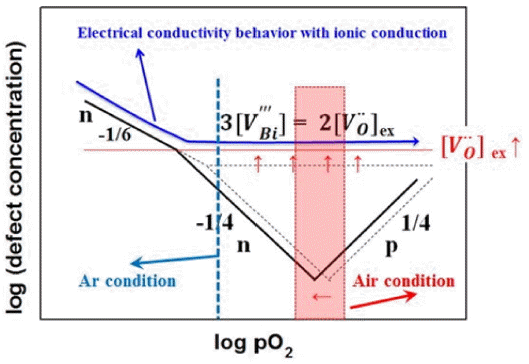
Schematic diagram of defect concentration (electrical conductivity) vs. oxygen partial pressure (pO2).
Equation (2) is the reaction formula for Bi volatility; Eq. (3) is the reaction formula for Fe transition, incorporating Eqs. (2) and (4). Thus, it can be explained that the ionic conductivity by oxygen vacancy (
Figure 7 shows the activation energy (Ea) for electrical conduction obtained for each specimen on an Arrhenius plot. The slopes of the Arrhenius plot were used to calculate the activation energy through the below equation.
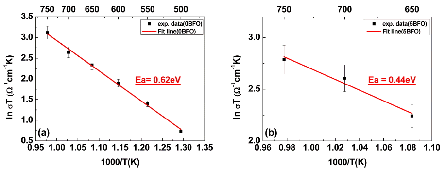
Arrhenius plots of electrical conductivity for air-quenched (AQ) (a) 0BFO and (b) 5BFO.
The activation energy values of 0BFO (Fig. 7(a)) and 5BFO (Fig. 7(b)) were 0.62 and 0.44 eV, respectively. These values are within the 0.4 – 1.0 eV activation energy range for oxygen vacancy movement for typical ABO3;23–25) thus, all the obtained activation energy results showed ionic conductivity behavior due to oxygen vacancy.
3.3. Seebeck Coefficient
In order to investigate the types of charge carriers, the Seebeck coefficient of 0BFO was measured as shown in Fig. 8. The measurements were conducted for in air and Ar gas atmospheres and a temperature range of 200 – 500°C. The Seebeck coefficient represents the thermoelectric power of the electron/hole carrier rather than that of the ion carrier. As shown in the oxygen partial pressure and electrical conductivity diagram of Fig. 6, the contribution of ionic conductivity was high in the measured oxygen partial pressure regime, and so the overall electrical conductivity was a constant value regardless of the oxygen partial pressure. However, minor carriers with low contribution actually coexist within the material and electron/hole conductivity transition (n-p transition) behavior was observed for the oxygen partial pressure of this regime. Such n-p transition was also easily observed in the results of Rojac et al.,19) which showed dominant electron/hole conductivity due to low oxygen vacancy concentration. In this study, the oxygen vacancy concentration for the measured 0BFO is relatively high, and so the n-p transition regime moves towards the low oxygen partial pressure because the ionic conduction by the oxygen vacancies is dominant. This movement of the n-p transition regime is also observed with temperature decrease. Thus, although the Seebeck coefficient measured in air atmosphere had a positive value (p-type) at low temperature, the Seebeck coefficient became negative or of n-type with temperature increase. A decrease in the absolute value of the Seebeck coefficient means that the charge carrier concentration increased. The relationship between the charge carrier concentration (n) and Seebeck coefficient (S) can be expressed by the Pisarenko expression, given in Eq. (7).26)
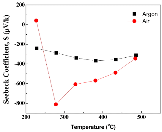
Seebeck coefficient (S) vs. temperature for 0BFO in different atmospheres (Argon and air).
Here, kB is the Boltzmann constant, h is the Planck constant, and
3.4. P-E Hysteresis Loop
Figure 9 shows the P-E hysteresis loop measurement results for 0BFO and 5BFO. The measurement results show that the remnant polarization (Pr) values for 0BFO and 5BFO were 91 μC/cm2 and 83 μC/cm2, respectively. These values were similar to the typical value of 90 – 100 μC/cm2 for BFO (single crystal). However, it is anticipated that the absence of complete saturation in the P-E hysteresis loop means that the hysteresis loop do not show capacitance but rather behavior due to current within the material or leakage current amount. The reason behind the low polarization value for 5BFO was thought to be the decrease in the leakage current compared to that of 0BFO due to the oxygen vacancy concentration decrease from excess Bi. Observation of the coercive field also revealed that the coercive field of 5BFO was greater than that of 0BFO. This proves the idea that the dielectric loss of 5BFO is small.

Room temperature ferroelectric hysteresis (P-E) loops of air-quenched (AQ) 0BFO and 5BFO.
3.5. Dielectric Constant and Dielectric Loss Measurement
Figure 10 shows the values of dielectric constant and dielectric loss of 0BFO and 5BFO. The measured dielectric constants shown in Figs. 10(a) and (c) indicate that the dielectric constant decreased as the measuring frequency (1, 10, 100 kHz) increased and the emerging Neel temperature (TN) range increased as the frequency increased. This frequency dependency clearly shows multiferroicity. The dielectric losses shown in Figs. 10(b) and (d) reveal large dielectric loss values starting from the low temperature range; the dielectric loss value for 0BFO, shown in Fig. 10(b), rapidly increased starting at a temperature lower than was the case for 5BFO, as shown in Fig. 10(d). This shows that dielectric loss occurs easily due to the higher oxygen vacancy concentration, which was compensated for Bi vacancy, of 0BFO compared to that of 5BFO. The high dielectric loss for BFO at a specific temperature and the lower frequency was in good agreement with the high ionic conductivity in the high temperature electrical conductivity results. This clearly shows that the oxygen vacancy concentration of BFO is high and transport is also high.
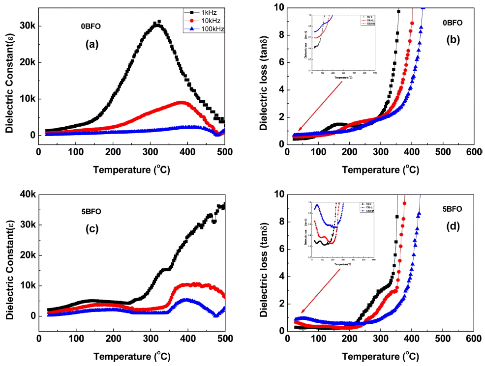
Temperature dependence of dielectric constant (ɛ) (a, c) and dielectric loss (tanδ) (b, d) for the air-quenched (AQ) 0BFO and 5BFO with measurement frequency from 1 kHz to 100 kHz.
4. Conclusions
In this study, the microstructure, electrical conductivity, and P-E hysteresis curve were investigated for X = (0, 0.05) Bi1+xFeO3±δ ceramics at various oxygen partial pressure atmospheres. The 0BFO and 5BFO ceramics were synthesized using the solid-state reaction method; to improve the microstructure and porosity, the synthesized ceramics were sintered using the two-step sintering method. High temperature electrical conductivity was measured to assess the main defect behavior of BFO. The high ionic conductivity due to oxygen vacancy compensation reaction (
Acknowledgements
This work was supported by the basic research program through the National Research Foundation of Korea (NRF), funded by Ministry of Education, Science and Technology (MEST) (2011-0030058) and the National Research Foundation of Korea (NRF-2015R1D1A1A01061479).