(K,Na)NbO3-based Lead-free Piezoelectric Materials: An Encounter with Scanning Probe Microscopy
Article information
Abstract
Environment-friendly (K,Na)NbO3-based (KNN) lead-free piezoelectric materials have been studied extensively in the past decade. Significant progress has been made in this field, manifesting competitive piezoelectric performance with that of lead-based, for specific application scenarios. Further understanding of the relationship between high piezoelectricity and microstructure or more precisely, ferroelectric domain structure, domain wall pinning effect, domain wall conduction and local polarization switching underpins the continuous advancement of piezoelectric properties, with the help of piezoresponse force microscopy (PFM). In this review, we will present the fundamentals of scanning probe microscopy (SPM) and its cardinal derivative in piezoelectric and ferroelectric world, PFM. Some representative operational modes and a variety of recent applications in KNN-based piezoelectric materials are presented. We expect that PFM and its combination with some newly developed technology will continue to provide great insight into piezoelectric materials and structures, and will play a valuable role in promoting the performance to a new level.
1. Introduction
Accumulation of electric charges proportional to an applied mechanical stress appear on the surface of certain crystalline materials was first experimentally observed by the Curie brothers in 1880, known as the direct piezoelectric effect. Correspondingly, these materials could develop a proportional deformation, expansion or contraction depending on the polarity, when subjected to an electric field, referred to as the converse piezoelectric effect.1) Piezoelectric materials have a functionality of interconverting electrical and mechanical energy, and hence have found themselves versatile in fields of information and communications, manufacturing automation, energy harvesting and medical diagnostics or, more specifically, sensors, transducers, motors and high voltage actuators, etc.2–12)
Currently, considering cost-effective material design, Pb(Zr,Ti)O3 (PZT) and its doped derivatives, are still the most commonly used materials in industry. However, these lead-based materials are hazardous to both human and environment. As a result, lead-free materials like (Bi0.5Na0.5)TiO3-BaTiO3 (BNT-BT)-based,13–19) (Ba,Ca)(Zr,Ti)O3 (BCZT)-based,20–25) polyvinylidene fluoride (PVDF)-based,26–31) BiFeO3-based32–35) and (K,Na)NbO3(KNN)-based36–45) materials have been studied in depth for years. Tremendous effort has been poured into research aimed at enhancing the performance and reliability of these materials, some of which even manifests great potential for transferring into industrial applications to substitute lead-containing ones in the near future.
Historically, lead has been successfully eliminated from some applications, including gasoline additives, ammunition, paints and allied products, and industrial inorganic chemicals, under the impetus of related laws and regulations. In order to encourage developing harmless lead-free materials to replace hazardous lead in PZT, restriction of the use of lead in piezoelectric electronic devices will also been implemented in the the European Union (EU), South Korea, China, etc. Two well-known legislations are the REACH (Registration, Evaluation, Authorization and Restriction of Chemical Substances) and the RoHS (restriction of the use of certain Hazardous Substances in electrical and electronic equipment) in the EU. Considering rigorous and thorough elimination of lead was technically impracticable, the applications using lead-containing material was temporarily exempted. However, these exemptions will be reviewed every five years. They will be terminated when feasible replacements are available. A report provided by European commission of 2016, which routinely assess the exemptions from the RoHS, recommend a shorter scheduled review period within 3 years, instead of 5 years.46)
Among all the lead-free candidates, KNN is endowed with a large piezoelectric coefficient and high Curie temperature Tc. Besides, KNN has also drawn much attention due to its well-balanced piezoelectric properties and better environmental compatibility. Moreover, inherent compatibility with low-cost base-metal electrodes like nickel, which is absent in PZT, has attracted intensive interests of industrial circles. Intensive research follows up since Saito et al. achieved a PZT-like piezoelectric coefficient in textured ceramics in 2004,47) mainly focusing on chemical modification, domain engineering and enhancement of temperature stability. KNN-based compositions have been intensively studied, contributing approximately half of the overall publications in the lead-free research field.2,8) A huge amount of improvement has been incrementally made in the field of KNN piezoelectric since the breakthrough in 2004. For example, Wu et al. developed a large piezoelectric coefficient d33 of 490 pC/N in new KNN-based compositions by introducing rhombohedral and tetragonal (R-T) phase boundaries.48) Wang et al. improved the temperature stability of piezoelectric strain with a variation of less than 10% from room temperature up to 175°C, attributed to the electrically enhanced diffused phase transition.40,49) In 2016, Wu et al. pushed the limit of d33 of KNN-based ceramics to as high as 570 pC/N, owing to the nanoscale strain domains and high density of ferroelectric domain boundaries.36)
Scanning probe microscopy (SPM) and its derivatives emerge as powerful tools to provide insight into the microscopic mechanisms, satisfying the growing demand for studying and modifying the properties and structures of materials at a nanoscale. Atomic force microscopy (AFM) and piezoresponse force microscopy (PFM) are two of the derivative imaging modes implemented on the basis of SPM. AFM has the function of imaging, force measurement and manipulation. As an extended concept of AFM, PFM probes electromechanical signal and provides abundant domain information from mesoscale down to nanoscale, has widely been applied in the research of piezoelectric, ferroelectric, and multiferroic materials.
Understanding of the origin of a high piezoelectric performance is necessary to push the performance limit scientifically. The relationship between properties and microstructure or more precisely, domain structures, is very important. The microstructure is expected to contribute considerably to the macroscopic piezoelectric response. Therefore, microstructural information, such as local symmetry, ferroelectric domain structure, domain wall pinning effect, domain wall conduction and local polarization switching all along are mainly focused in piezoelectric and ferroelectric communities. With the help of PFM, valuable information on static and dynamic properties could be provided. Thus, it is quite a suitable time to review the recent advancement of KNN materials with the assistance of PFM. In this review, we will briefly introduce the fundamentals of PFM, and its applications in recent development of KNN materials.
2. Fundamentals of Strain-based Scanning Probe Microscopies
In 1986, Binnig, Quate and Gerber invented Atomic Force Microscope (AFM), on the basis of the concept of Scanning Tunneling Microscope (STM).50) Taking advantage of interatomic force, surface topography with a high resolution at atomic level could be detected. The application was later extended to not only conductors and semiconductors, but also insulators. Typical AFM experimental setup consists four core components: (1) a cantilever with a probing tip that serves as a force sensor and optical lever; (2) a four-quadrant photodiode that measures cantilever deflection by detecting a reflected laser signal; (3) a scanner driven by piezoelectric actuator that moves the sample relatively to the cantilever in the plane during scanning process; and (4) a data acquisition and control unit. A force resulted from the interaction between the probing tip and the sample surface could be either attractive or repulsive, due to interatomic force. During calibration procedure, this force will be set to a given value manually by adjusting the height distance between the tip and the surface, depending on experimental conditions. Height position of the cantilever can be determined with reflected laser. During scanning, the scanner moves the sample back and forth. As the sample moves, the photodiode detector can measure signal variations due to the fluctuating height of the sample surface. Then, these signals will be saved in a square matrix, and a 2-D visualization of surface topography can be provided. Constant force mode and AC mode are two commonly used imaging modes in AFM. As shown in Fig. 1, the Z-axis position of the cantilever is calibrated to keep the deflection constant at the set point as the tip scans over the surface with contact feedback on. While the amplitude will be constant at the set point with AC feedback on. AC mode has an advantage of a higher spatial resolution as the tip vibrates at resonance frequency. Therefore, AC mode is more favored for testing a sample with rough surface to further amplify the signals.
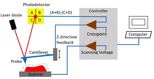
Schematic illustration of AFM measurement mechanism.
PFM is employed to investigate ferroelectric domains on the basis of AFM. The working principle is illustrated in Fig. 2, which has much in common with that of AFM.51–55) The difference is that an AC voltage is applied on a sample surface with a conductive probing tip in contact mode. Normally, polarization direction varies in un-poled ferroelectric domains. Domains with different polarization direction exhibit various strain under a same electrical excitation. If the polarization is uniformly out of plane, a normal strain develops, causing up or down displacement of the tip, which can be detected with a laser spot reflected on photodiode, as shown in Fig. 3. While a shear stress will arise if the polarization direction is in plane, leading to a left or right displacement of the tip. Furthermore, displacement of the laser spot is proportional to the magnitude of the strain. Thus, not only polarization direction but also the amplitude of the piezoelectric response could be determined.
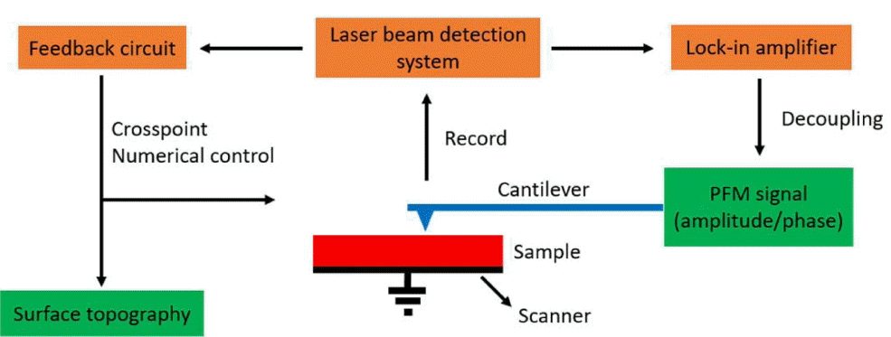
Imaging mechanism of PFM.
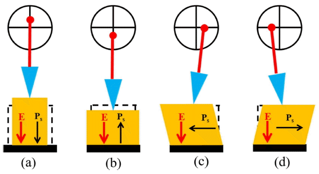
Schematics of (a–b) vertical and (c–d) lateral PFM.
The Vtip voltage applied to the tip consists of a DC component Vdc and an AC component
Sample develops a deformation under the Vtip voltage, due to piezoelectric effect. Take c domain for example, tip produces a displacement z at longitudinal direction, could also be divided into DC and AC two parts:
When the frequency of AC voltage is at resonance of domain, z could be expressed as:
The amplitude of z reflects d33 of the material and the phase ϕ is related to the polarization orientation of the domain. As the tip contacts with the sample surface at a fine point with a size comparable to the tip apex radius (less than 10 nm), the detected signal is the piezoelectric response of superficial domains with a thickness less than 10 nm. Besides, crystallographic orientation and contact condition can also influence the response. Therefore, it should be clarified that this d33 is an effective parameter or more precisely, the d33 is equal to the out-of-plane strain induced by the longitudinally applied voltage, denoted as Smax/Emax. Similarly, the in-plane piezoelectric amplitude can be evaluated as an effective piezoelectric coefficient d15.
The frequency of AC voltage is fixed at a value near resonant frequency manually to amplify piezoelectric signal during scanning. However, resonant frequency varies with the surface topography of the sample. It is more likely to obtain a response with a considerable offset in both amplitude and phase if the frequency is a fixed single value. By introducing Dual Frequency Resonance Tracking (DART), resonant frequency could be traced and every single testing point could be experimentally conducted at resonant frequency.28)
3. Applications of PFM
In this section, we focus on applications of PFM for study KNN-based piezoelectric materials.
3.1. Domain morphology characterization
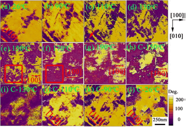
Normally, macroscopic performance of a material depends strongly on its microstructures. Ferroelectric domain is a micro-region that possesses a spontaneous electric polarization. It is well accepted that the piezoelectric performance is closely related to the domain morphology.57–59) For example, domain wall motion and domain rotation have significant influence on the dielectric and piezoelectric performance of ferroelectric materials, contributing as much as 70% of the macroscopic response.60) It is therefore necessary to investigate the evolvement of domain structure, serving as a good indicator to the macroscopic electromechanical response. Fig. 4 shows in situ lateral piezoresponse force microscopy (LPFM) images of 0.96(K0.4Na0.6)(Nb0.96Sb0.04)O3-0.04Bi0.5-K0.5Zr0.85Sn0.15O3 (KNNS-BKZS) measured at different temperatures (28, 50 and 100°C). Fig. 4(a) – (c) are the piezoresponse amplitude and Fig. 4(d) – (f) are the piezoresponse phase. Regular micro-sized domains and abnormally fine domains with a nanoscale coexist at room temperature (RT), marked as region ‘a’ and region ‘b’, respectively. Considering that rhombohedral-tetragonal (R-T) phase transition temperature TR-T is around RT, the existence of two different types of domains may be due to the R-T phase coexistence. However, domain boundaries become obscure as the temperature rises to 50°C, as shown in Fig. 4(b) and (e). A moderate decrease in piezoresponse is observed for nano-sized domains in both amplitude and phase image, while the piezoresponse of micro-sized domains remains almost unchanged. The micro-sized domains show less temperature dependence than that of the nano-sized domains. A phase transformation from rhombohedral to tetragonal occurs as the temperature increases to 50°C and a restructuring of domains occurs, showing different temperature stability of the two types of domains. As the temperature increases up to 100°C, piezoresponse amplitude greatly declines, in both types of domains. Nearly all the domains have vanished and the remaining domains are found to have very blurred boundaries. Similar temperature-dependent behaviors of both types of domains observed between 50°C and 100°C are due to the existence of a single tetragonal phase during the whole temperature range.
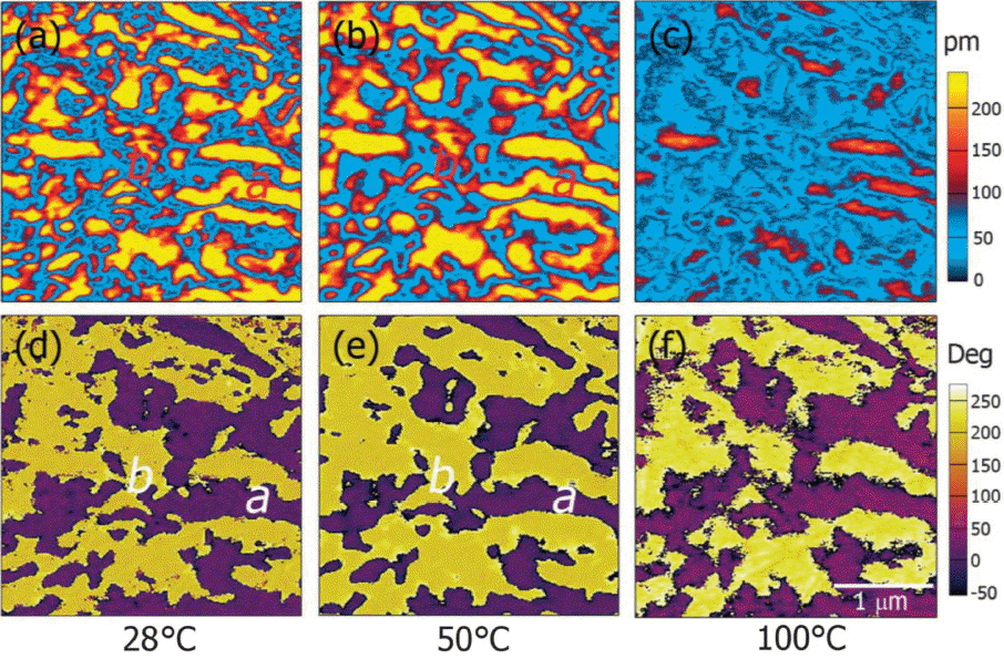
The square root of domain wall energy is proportional to its domain size. The nano-sized domains possess extremely low domain wall energy and therefore are sensitive to electric field stimulation, contributing to the extrinsic piezoelectric effect. Theoretically, temperature-dependent macroscopic piezoresponse depends on the transformation of domain morphology at different temperatures. At RT, extrinsic effect contributed by nano-sized domains leads to the optimal piezoelectricity. Upon heating to 50°C, a portion of the nano-sized domains diminishs, leading to a slight decrease in piezoelectricity. When the temperature increases up to 100°C, disappearance of both micro-sized domains and nano-sized domains leads to a dramatic decline in piezoelectric property d33.
Besides manifesting in modifications of piezoelectric tensor, ferroelectric phase transition involves in the variation of spatial domain arrangement as well.61) Namely, domain evolution is associated with a phase restructuring and a continuous reordering of domains upon heating and cooling. Herein, an investigation into a Li-doped KNN epitaxial thin film by using PFM, exhibiting ferroelectric phase transition, is reviewed.
In-plane (IP) PFM amplitude and phase evolution with temperature are shown in Fig. 5 and Fig. 6, respectively. In the beginning, stripe domains with domain walls along [110] direction are visible in the (001) plane. Both the amplitude and phase patterns remain unchanged in the temperature range between 26 and 90°C. Twisted domain walls show up at 110°C, marked by red arrows in Fig. 5 and Fig. 6, manifesting the beginning of domain movement. Distinct domain wall movement and obvious variation in domain structure occur in both amplitude and phase patterns at 130°C and 150°C. Stripe domains are invisible at 130°C, with considerable shrinkage in yellow contrast in the phase pattern simultaneously. A new developed direction of domain wall along [100] direction emerges at 150°C, marked by red dashed lines in Fig. 5 and Fig. 6, indicating formation of a new phase. The direction maintains along [100] upon heating to 190°C. However, there are many small domains merge into larger domains, which visibly shown in a red-square-highlighted region in Fig. 6. Then, upon cooling, a notable change occurs in the temperature range between 130°C and 110°C, where a domain wall with the direction along [110] reappear at 110°C. The amplitude and phase patterns gradually evolve with the decline of temperature and almost reset to the former configuration prior to the heating run. This experiment clearly demonstrates the feasibility of capturing the domain wall motion upon heating or cooling, and this may provide a better prediction of macroscopic temperature-dependent performance of materials.

3.2. Local poling
By applying a DC voltage to the tip when scanning at a certain point of the surface, local poling could be realized in ferroelectric sample. Meanwhile, reversely local poling of ferroelectric domain occurs by varying the magnitude and the direction of DC voltage. Two samples with different compositions are compared, as shown in Fig. 7. To begin with, a negative voltage of −15 V and −10 V are applied to the tip during scanning of a 4 × 4 mm2 region of sample A and B, respectively, which are large enough to induce complete polarization alignments. Relatively bright region represents a uniform upward (out-of-plane) polarization. Then, different positive voltages are applied to four squares of 1 × 1 μm2 in both samples. Difference of the magnitude of voltages in two samples is purposely designed to construct a symmetrical poling condition in negative and positive directions.
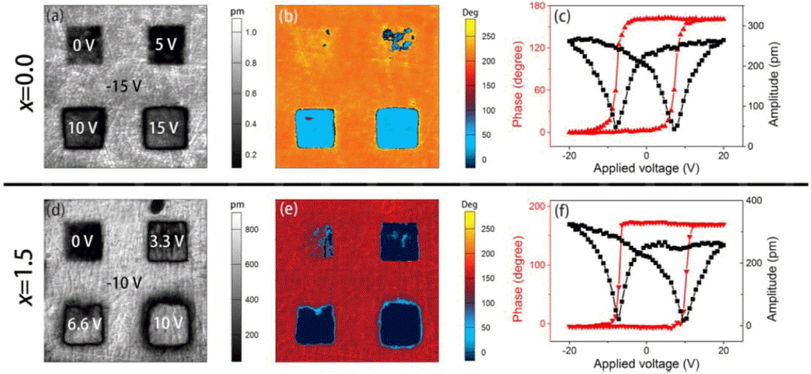
Poling behavior of KNN-BLT-BZ-xMn (x = 0 and x = 1.5). Out-of-plane images after poling with different electrical voltages, as illustrated in parts a and d, where the areas of whole testing region and 4 squares are 4 × 4 μm2 and 1 × 1 μm2, respectively. Reprinted with permission from Ref. [42], J. Am. Chem. Soc., 2017, 139 (10), 3889–3895. Copyright (2017) American Chemical Society
For sample A, domains are almost unchanged in the 0 V region, showing the collective polarization vector is still upward.63–65) Under a voltage of 5 V, only partial domains have been reversed, showing an insufficient electric field to induce complete domain switching. Finally, under a voltage of 10 V, all the domains have been completely reversed and the polarization vector is uniformly downward. Compared with sample A, a lower voltage of 3.3 V is enough to induce considerable domain reversal of sample B. The reduced voltage to invert collective polarization orientation manifests enhanced domain mobility in sample B, which is regarded as a key factor to have improved the macroscopic electromechanical performance.42)
3.3. SS-PFM
Local polarization switching spectroscopy is employed to verify ferroelectricity on the nanoscale. Furthermore, it is possible to accomplish domain reversal by applying a high DC voltage to the probing tip, known as Switching Spectroscopy PFM (SS-PFM). As the piezoresponse-voltage hysteresis loops are obtained during periodical changes, piezoelectric response, coercive field and internal bias field could be determined.
For a local switching testing, resonance frequency should be determined first by tuning at a certain point on the sample surface, using an AC field. Then, a mixed voltage input of a stepwise increasing DC voltage with a superimposition of an AC voltage, which has been determined during tuning, is applied to the conductive tip. The voltage loading as a function of time is illustrated in Fig. 8. The “on” state and “off ” sate refer to the status of DC loading. DC voltage is used to polarize the sample and reverse the domains. While AC voltage, with a resonant frequency, is used to amplify piezoelectric signal. Due to the interference between electrostatic effect and piezoelectric response, typical amplitude-voltage hysteresis loop acquired during on-state is quite different from that of off-state, which is rarely addressed.51,66) Piezoelectric signal is usually adopted during the “off” state with only an AC voltage applied to the conductive tip.
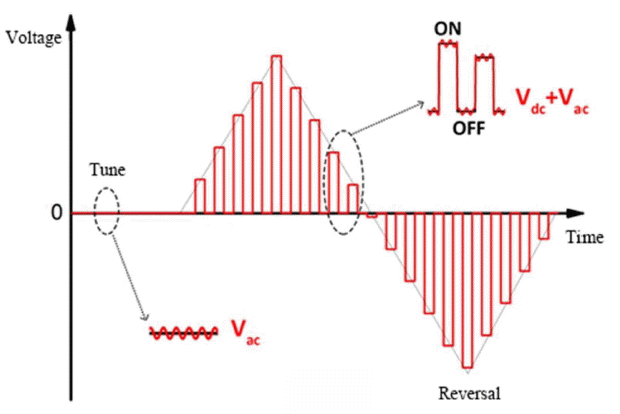
Schematic diagram of waveform loaded during SS-PFM measurement.
Typical amplitude-voltage and phase-voltage hysteresis loops obtained through the switching measurement are shown in Fig. 9. Amplitude values obtained at zero and maximum voltage, divided by the magnitude of the AC voltage (Amplitude[0]/AC voltage and Amplitude[max]/AC voltage) is regarded as the local effective piezoelectric coefficient d33 and dmax, respectively. The amplitude at maximum voltage stands for deformation of material in polarized state, which could be expressed as:
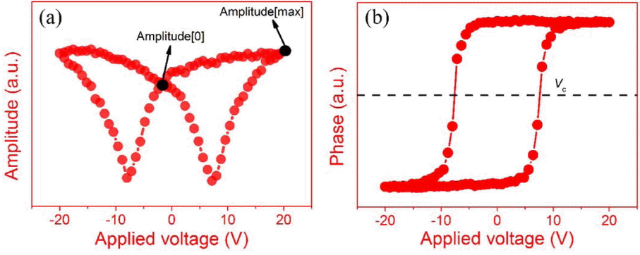
(a) Typical piezoresponse hysteresis loop under “off” state and (b) phase-voltage chart.
where Vac is the magnitude of applied AC voltage during testing and Q is the quality factor, representing the magnification times/enlargement factor during testing. Thus, it is possible to calculate effective piezoelectric coefficient d33. Generally, Q value ranges from 10 to 100 and could be automatically calculated in DART mode.
It is noted that the local effective piezoelectric coefficient d33 and dmax measured in different experiment cannot be compared directly as they are highly correlated with the tip-sample contact stiffness. Furthermore, for nano-scale materials like nanofibers, nanorods and nanowires, it is almost impossible to characterize piezoelectricity quantitatively when compared to bulk materials, due to a significant size difference. However, effective qualitative measurement is still in need. A qualitative comparison of piezoelectric response achieved by introducing a quality factor Q during the tuning process will be discussed.
Resonance frequencies of KNN nanorods (NRs) with different K/Na ratio are listed in Fig. 10. Difference in resonance frequencies is due to impacts of varying contact stiffness. By extracting the ratio of resonance frequency and the full width of the amplitude peak at about 70% of the peak value, the quality factor Q could be calculated.68) The variation of resonance peak as well as calculated Q value with the K/Na composition is plotted in Fig. 10(b). The quality factor Q varies from 67 to 89 under a driven voltage of 3 V, revealing the importance of excluding the influence of contact on amplitude data. By altering the driven voltage from 1 V to 6 V at a step of 1 V, a series of the amplitude data is obtained. It is noted that more than 15 measurements were taken for a given voltage. The dependence of tuning amplitude on the driven voltage could be linearly fitted, manifesting the piezoelectric nature.

(a) Vibration amplitude versus frequency near resonance gathered from KNN NRs with different compositions. (b) Variation of resonance frequency and calculated quality factor Q. (c) Tuning amplitudes and the linear fittings versus the applied AC voltage. Reproduced from Ref. [67] with permission from The Royal Society of Chemistry.
3.4. Domain dynamics study
While lots of attempts have been devoted to improving piezoelectricity of KNN materials by doping or unconventional sintering, there are few studies about the dynamics of domain nucleation and growth in KNN piezoelectric materials. Piezoelectric response includes the lattice displacement and domain wall motion, known as the intrinsic effect and the extrinsic effect, respectively. Thus, it is important to investigate on domain dynamics to shed light on the underlying mechanism and therefore, to further enhance piezoelectricity.
By applying a DC voltage (writing voltage) to the tip at a certain point of the surface of a ferroelectric sample, PFM could be used to write artificial domains as desired. By stepping up the writing voltages with a fixed pulse duration and mounting the pulse duration with a fixed writing voltage, it is possible to investigate the dependence of some featured parameters on the tip voltage or the pulse duration, as shown in Fig. 11.69–71) Domains can easily be distinguished, due to significant color contrast. The voltage-induced domain is the brightest part at the center of the image. As the amplitude and the duration increase, the brightest area gradually enlarges. The domain size and domain wall velocity ν are calculated, according to the square root of the calculated area of the domains and the growth time of domains.
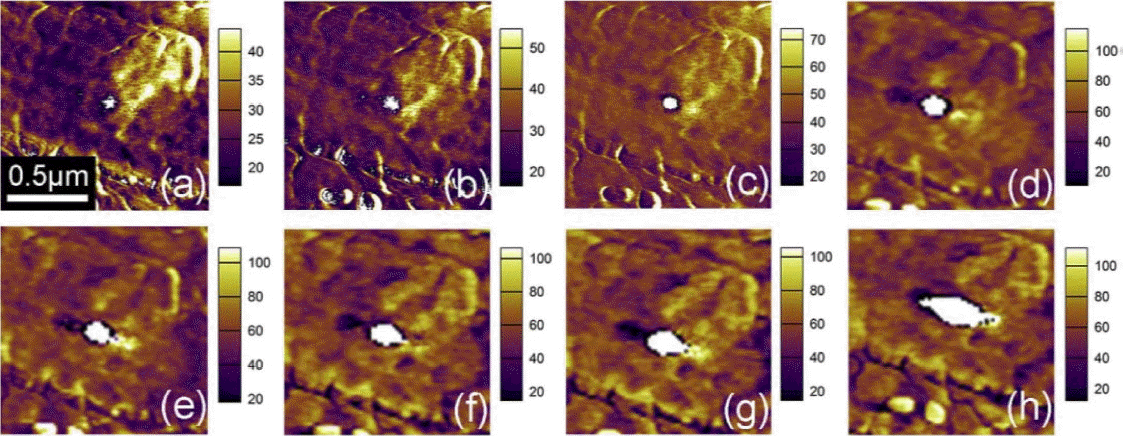
The domain size possesses a linear relationship with the pulse voltage and the dependence of the domain size on the pulse time duration is more complex than the logarithmic one, as shown in Fig. 12. Besides, the domain wall velocity follows a power law on the domain size with a small exponent μ of 0.10, implying a strong pinning effect caused by point defects. This approach leads to a better understanding of the underlying mechanisms that affects the piezoelectric performance of KNN materials, and prove the importance of PFM in local studies of piezoelectrics.
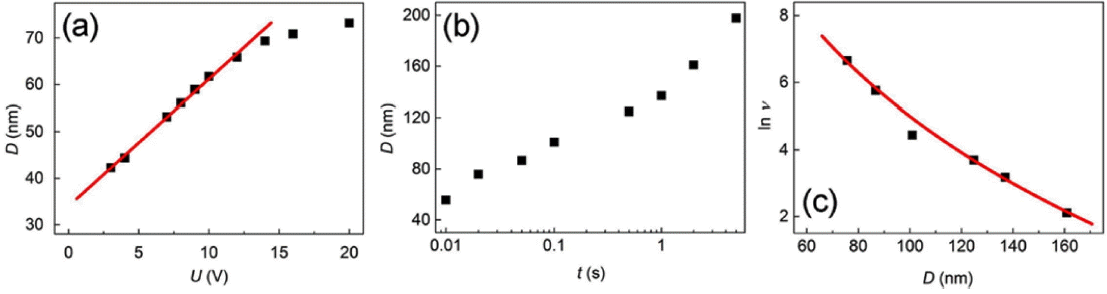
The dependence of (a) the domain area on the tip voltage, (b) the domain size on the pulse duration, and (c) the domain wall velocity on the domain size. The lines represent fitting results. Reprinted from Ref. [69], Ceramics International 43 (2017) 9538–9542. Copyright (2017), with permission from Elsevier.
3.5. Tip-enhanced phonon Raman spectroscopy
Despite a powerful technique to obtain the amplitude and phase contrast in ferroelectric materials, PFM is an indirect way to determine the spatial electric polarization, especially for the cases where several equivalent orientations of the spontaneous polarization occur. A general concept for combining optical spectroscopy with scanning probe microscopy emerged recently, which is known as tip-enhanced Raman scattering (TERS).72) Due to the spontaneous polarization, ferroelectric materials develop anisotropic optical interactions, where optical response couples to the ferroelectric lattice distortion or the resulting electronic properties variation. Recently, TERS has been adopted to reveal intrinsic ferroelectric domains of BaTiO3 nanorods by probing different transverse optical phonon modes.73) The research shows that although the nanorods are smaller than typical ferroelectric domains in size, they are not single domain state. For materials at nanoscale, an increase in surface to volume ratios and the associated increasing role of the surface free energy plays in ferroelectric ordering may induce finite size effects. TERS has only been conducted in BaTiO3 system so far, an extension to KNN system will afford an insight into the ferroelectric domain mechanisms from a new prospective.
4. Conclusions
We introduce the fundamentals of PFM, and its applications in recent development of KNN materials. We expect that PFM will provide new insight into functional materials like piezoelectrics in the years to come. A combination with newly developed technology will certainly pour strong vitality and vigor into the piezoelectric and ferroelectric field.
Acknowledgements
This work was supported by National Nature Science Foundation of China (Grants no. 51572143, 51332002), the Tsinghua University Initiative Scientific Research Program (Grant no. 20131089230), and Science Challenge Project. X. C. acknowledges the support by 973 Program (Grant no. 2015CB654604) and Beijing Science and Technology Program (Grant no. Z161100003016015).