Preparation of Gas Sensors with Nanostructured SnO2 Thick Films with Different Pd Doping Concentrations by an Ink Dropping Method
Article information
Abstract
Pd-doped SnO2 thick film with a pure tetragonal phase was prepared on patterned Pt electrodes by an ink dropping method. Nanostructured SnO2 powder with a diameter of 10 nm was obtained by a modified hydrazine method. Then the ink solution was fabricated by mixing water, glycerol, bicine and the Pd-doped SnO2 powder. When the Pd doping concentration was increased, the grain size of the Pd-doped SnO2 thick film became smaller. However, an agglomerated and extruded surface morphology was observed for the films with Pd addition over 4 wt%. The orthorhombic phase disappeared even at a low Pd doping concentration and a PdO peak was obtained for a high Pd doping concentration. The crack-free Pd-doped SnO2 thick films were able to successfully fill the 30 μm gap of the patterned Pt electrodes by the optimized ink dropping method. The prepared 3 wt% Pd-doped SnO2 thick films showed monoxide gas responses (Rair/RCO) of 4.0 and 35.6 for 100 and 5000 ppm, respectively.
1. Introduction
Semiconductor sensors have drawn much attention in various applications for detecting noninflammable, toxic, and odorless gases, because of the low price, small size, manufacturing convenience, and low gas detection limit.1–3) Recently, many metal oxides are being investigated as toxic semiconductor sensor materials. SnO2, an n-type semiconductor having a band gap 3.62 eV, is one of the most studied semiconductor gas sensor materials because of its advantages of simple structure, high chemical stability, and rapid response to gas.4) Fabrication of a good semiconductor gas sensor requires not only that the sensor have high response to the gas to be detected but also the solving of problems such as drift of response during long-term operation and low selectivity in the presence of many kinds of gases. Doping of a rare metal oxide or a precious metal has been studied as a convenient method of solving such problems of semiconductor gas sensors. Pd, which has been intensively studied along with Pt, is used as an effective catalyst that lowers the activation of oxygen molecule decomposition. 5–8)
Nanostructures having a particularly high surface-area-to-volume ratio are appropriate for use gas sensor structure because gas is highly likely to be adsorbed and desorbed in the structure.9–11) Various methods are employed for the deposition of a nanostructured SnO2 film, including sputtering, sol-gel spin coating, chemical vapor deposition (CVD), laser ablation technique, evaporation, and wet chemical synthesis. Since these methods require a relatively high temperature for the formation of a nanostructured SnO2 film, additional patterning through photolithography is needed to fabricated the gas sensor device. Ink printing, because of advantages such as vacuumless process, low price, low material loss, and high throughput, originally used for printing in offices, has been extensively studied as a device fabrication method that does not require patterning.
For the realization of a semiconductor gas sensor employing a nanostructured Pd-doped SnO2 thick film, the present study focused on the following three issues. The first was to prepare, through an improved hydrazine method, a nanostructured, Pd-doped SnO2 powder from raw materials, Sn chlorides, and Pd chlorides. The second was to investigate the effect of the quantity of Pd doping on the surface shape of the nanostructure, crystallographic structure, and wettability on a Pt electrode when a thick film is formed on a patterned Pt electrode by ink dropping with the previously prepared Pd-doped SnO2 powder. The last issue was to measure the response to monoxide gas of the Pd-doped SnO2 thick film formed on the patterned Pt electrode.
2. Experimental Procedure
Figure 1 is a schematic diagram showing how to synthesize pure and Pd-doped nanostructured SnO2 powder by the hydrazine method. The starting materials used for the preparation of the pure SnO2 powder were tin chloride dihydrate (SnCl2·2H2O, Sigma Aldrich) and hydrazine hydrate (N2H4·H2O, Sigma Aldrich). Palladium(II) chloride (PdCl2, Sigma Aldrich) was used to prepare the Pd-doped SnO2 powder, in which the Pd doping concentration was controlled in a range from 1 wt% to 5 wt%.
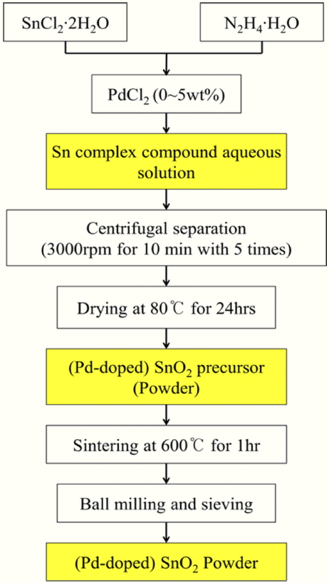
Process flow diagrams for nano-structured pure and Pd-doped SnO2 powder using hydrazine method
First, these raw materials were mixed and stirred for 24 h at room temperature to produce an aqueous solution-based and Sn-based inorganic complex compound. The resulting solution was diluted with distilled water five times using a centrifugator at 3000 rpm for 10 minutes each time. Then, the resulting solution was thermally treated at 80°C for 24 h to obtain white precipitate powder. The powder type precursor was sintered at 600°C for 1 h in air atmosphere to obtain SnO2 powder as the final product. The overall chemical formula used in the hydrazine method for preparing the SnO2 powder is expressed as Equation (1)12–15):
To prepare the SnO2 ink solution, an aqueous glycerol solution was prepared by mixing deionized water and glycerol at a ratio of 1:1. After adding 1 wt% bicine as a dispersing agent, the resulting solution was sonicated for 15 minutes. The pure or Pd-doped SnO2 powder prepared previously was added at a ratio of 2 wt%, and the resulting solution was sonicated for further 15 minutes to obtain the final ink solution.
The prepared ink solution was dropped on a patterned Pt electrode using a micropipette. Using a lift-off process, a 100 nm-thick Pt bottom electrode was patterned on the SiO2/Si substrate and the gap between the electrodes was fixed at 30 μm. The volume of one ink drop was controlled at 70 μl. The ink drops were dried at 300°C for three hours to remove organic substances and water included in the ink. Then, after one hour of thermal treatment was performed at 600°C to increase the contact with the electrode, an SnO2 thick film was formed.
The thermal behavior of the SnO2 precursor previously obtained by mixing the raw materials, and the temperature of the transformation to the SnO2 phase, were observed using a thermo gravimetric and differential thermal analyzer (TG and DTA, Netzsch DSC200F3). The crystallographic structure of the SnO2 thick film was determined using an X-ray diffractometer (XRD, Rigaku D/MAX-2200/PC), wherein the Bragg-Brentano geometry (θ-2θ) mode using Cu Kα radiation was employed in X-ray crystallography. Surface images of the SnO2 thick film were obtained using a a field emission scanning electron microscope (FESEM, Hitachi S-4700). The area of the entire thick film pattern formed on the electrode was verified using an optical microscope (OM, Sometech SV-55).
The gas-sensing characteristics were measured according to the variation of the resistance of the SnO2 thick film, which was located between electrodes at a measurement temperature fixed at 300°C, by varying the CO gas concentration from 100 ppm to 5,000 ppm. While gas of varying concentration was being injected via a mass flow controller (MFC) into the chamber in which the sensor sample was located, the variation of the electric resistance was sensed according to the voltage measured at a constant current of 1 μA. The gas response was defined as the ratio of the electric resistance, Rair/Rgas, wherein Rair and Rgas denote the electric resistance measured in air atmosphere and in the target gas atmosphere, respectively.
3. Results and Discussion
Figure 2 shows the TG and DTA analysis results for the prepared SnO2 precursor powder. This study was performed to determine an appropriate sintering temperature. The TG curve showed two major changes in the mass in the temperature range between 225°C and 285°C. The increase of the mass might have been due to oxidation, while the decrease of the mass might have been due to decomposition. The DTA curve also showed large exothermic reaction peaks at the points where major mass changes were found in the TG curve. In addition, the DTA curve showed that the mass continuously decreased as the temperature was increased up to 600°C. The sintering temperature was finally determined to be 600°C, because no noticeable endothermic or exothermic reaction peak was observed until this temperature, while the decrease of the mass was saturated to some extent. Sintering at a higher temperature may have a negative effect on the gas-sensing characteristics, because the crystal size of the nanostructure may increase due to crystal grain growth of the SnO2 powder.

TG and DTA curves for SnO2 precursor powder according to temperature.
Figure 3 shows the XRD pattern of the SnO2 thick films formed by dropping onto the Pt electrodes the ink prepared using the aqueous glycerol solution of the previously prepared pure or Pd-doped SnO2 powders. The Pd-doping concentration was varied from 0 wt% (pure SnO2) to 5 wt%. The final sintering temperature was 600°C, and the sintering duration was three hours. The main phase of the SnO2 thick films was a tetragonal phase, regardless of the doping concentration. The tetragonal phase of the SnO2 thick films was confirmed because the XRD pattern was almost consistent with the standard XRD peaks of JCPDS 71-0652 (standard tetragonal SnO2, ICSD data); this pattern is also shown in Fig. 2 for comparison. The pattern of the pure SnO2 thick film included a peak corresponding to an orthorhombic phase, which disappeared as Pd was doped. When the Pd-doping concentration was over 4 wt%, a peak corresponding to PdO appeared. In addition, as the Pd-doping concentration increased, the width of the peak was gradually increased.
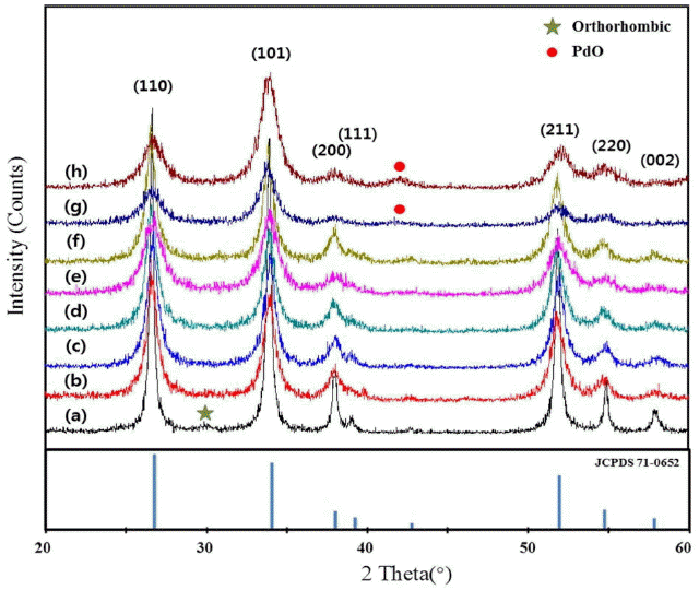
XRD patterns of (a) Pure SnO2, (b) 1 wt% Pd SnO2, (c) 1.5 wt% Pd SnO2, and (d) 2wt% Pd SnO2, (e) 2.5 wt% Pd SnO2, (f) 3 wt% Pd SnO2, (g) 4wt% Pd SnO2, and (h) 5 wt% Pd SnO2 thick films formed by ink dropping method: Volume of an ink drop, 70 μl; Drying temperature, 300°C; Sintering temperature, 600°C.
In the XRD pattern, the width of the peaks probably increased because the size of the crystal grains gradually decreased as the Pd-doping concentration increased. The relation between the crystal grain size and the XRD peak width is given in the Debye-Scherrer equation, Equation (2):
where d denotes the mean size of the crystal grains, k the Debye-Scherrer constant (0.89), λ the X-ray wavelength, β the full width at half maximum line broadening in radians, and θ the Bragg diffraction angle.
Table 1 shows the mean size of the crystal grains calculated using Equation (2), with the XRD pattern shown in Table 1. The mean crystal grain size of the pure SnO2 thick film was 32.3 nm. As the Pd-doping concentration increased, the crystal grain size of the pure SnO2 thick film gradually decreased to 8.8 nm at 5 wt% of the Pd-doping concentration. The decrease of the crystal grain size depending on the Pd-doping concentration increase may be due to the Pd-doping components, which inhibit the growth of crystal grains by preventing the movement of the crystal grain boundaries during the growth of the SnO2 crystals.16)
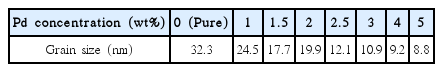
Grain Size of Ink Dropped SnO2 Thick Films with Pd Doping Concentration Determined from XRD Peak Broadening and Debye-Scherrer Equation
Figure 4 provides SEM images of the SnO2 thick films at the different doping concentrations shown in Fig. 3. As the doping concentration increased, from the pure, un-doped sample to the 3 wt% Pd-doped SnO2 thick film, the crystal grain size decreased and the surface shape became uniform. However, at Pd-doping concentrations of 4 wt% or higher, the nanocrystals coalesced with each other even to the degree of forming extrusions.
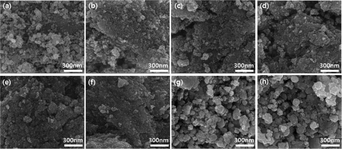
SEM surface images of (a) Pure SnO2, (b) 1 wt% Pd SnO2, (c) 1.5 wt% Pd SnO2, and (d) 2 wt% Pd SnO2, (e) 2.5 wt% Pd SnO2, (f) 3 wt% Pd SnO2, (g) 4 wt% Pd SnO2, and (h) 5 wt% Pd SnO2 thick films formed via ink dropping method.
Figure 5 provides microscopic images revealing the overall configuration of the thick films formed by inking dropping on the patterned electrodes. As the Pd-doping concentration was increased, the surface color became darker due to the effect of the heavy Pd metal. All the SnO2 thick films filled the 30 μm gap between the Pt electrodes well, without cracks or spreading. The area of the SnO2 thick films formed on the Pt electrodes was not significantly dependent on the Pd-doping concentration. The area of the SnO2 thick films formed using ink drops of 70 μl was in a range from 1.8 to 2.5 mm2. This may be because the wettability of the SnO2 ink on the Pt electrode was not significantly dependent on the Pd-doping ink. Previous report showed that the addition of Pd decreased the adherence to the bottom substrate.17,18) In the present study, however, no adherence problem due to the addition of Pd was found between the SnO2 thick films and the electrodes, even without any particular surface treatment. Therefore, ink dropping may be considered as an effective thick film deposition method for forming a Pd-doped SnO2 thick film on a Pt bottom electrode.
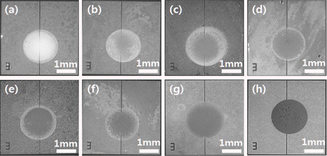
Optical images of (a) Pure SnO2, (b) 1 wt% Pd SnO2, (c) 1.5 wt% Pd SnO2, and (d) 2 wt% Pd SnO2, (e) 2.5 wt% Pd SnO2, (f) 3 wt% Pd SnO2, (g) 4 wt% Pd SnO2, and (h) 5 wt% Pd SnO2 thick films formed by ink dropping method.
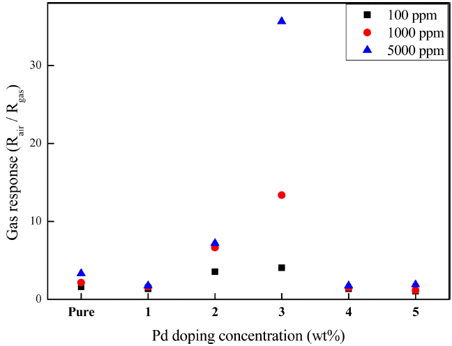
Figure 6 shows the carbon monoxide gas response of the SnO2 thick films formed on the Pt electrodes shown in Fig. 5 at different doping concentrations. Since SnO2 is an n-type semiconductor, when a reducing gas, such as carbon monoxide, enters into the sensor, it is adsorbed into the nanostructured SnO2 surface, and reacts with an oxygen atom; the oxygen atom is desorbed and an electron is introduced to the inside of the thin film, reducing the electric resistance. Hence, a large value of the gas response, expressed as Rair/Rgas, means an efficient gas sensor. The initial electric resistance, Rair, was in the range of 2 to 5 MΩ, and did not show a distinctive dependence on the Pd-doping concentration. The gas response of all the samples increased as the CO gas concentration increased. As the Pd-doping concentration increased to 3 wt%, the gas response strongly increased, with the highest gas response at 3 wt%. The gas response value was 13.0 at 1000 ppm and 35.6 at 5000 ppm.
Gas response of SnO2 thick films for various CO concentrations with Pd doping amount.
However, the gas response decreased at Pd-doping concentrations equal to or higher than 4 wt%. Two possible reasons for this finding may be assumed on the basis of previously determined analytical results. The first possible reason is related to the formation of the PdO phase, which occurred at Pd-doping concentrations equal to or higher than 4 wt%. Since PdO is an p-type semiconductor, unlike SnO2 which is an n-type semiconductor, the electric resistance of PdO is increased by a reducing gas, lowering the gas response.19) The second possible reason is related to the generation of macro-sized particles via the coalescence of nanostructure particles observed on the surfaces Pd doped at concentrations equal to or higher than 4 wt%. In such a case, as the effective surface area for the response to gas particles decreases, the electrical connectivity between the macro-sized particles decreases, resulting in a poor gas response.9) Further studies will be conducted to determine the mechanism of the gas response decrease at high Pd-doping concentrations.
4. Conclusions
In the present study, nanostructured pure and Pd-doped SnO2 powder was prepared using an improved hydrazine method, and an ink was prepared by mixing the SnO2 powder with an aqueous glycerol solution. The prepared ink, showing appropriate wettability on bottom Pt electrodes, was dropped on patterned Pt electrodes to effectively form thick films for the fabrication of a gas sensor. In the SnO2 thick films deposited on the Pt electrodes, the crystal grain size decreased as the Pd-doping concentration increased. However, at Pd-doping concentrations equal to or higher than 4 wt%, the XRD results show a peak corresponding to the PdO phase, and the surface showed coalescence of nanostructure crystal grains. The most uniform surface shape was found at the Pd-doping concentration of 3 wt%, at which the calculated mean crystal grain size was 10.9 nm. The best carbon monoxide gas response value was found in the SnO2 thick film having the Pd-doping concentration of 3 wt%. The Rair /Rgas value of the SnO2 thick film was 4.0 at the gas concentration of 100 ppm, and as high as 35.6 at 5000 ppm. The Pd catalyst-doped SnO2 thick film deposition based on ink dropping method suggested in the present study does not require additional patterning, does not produce microcracks, and shows excellent film adherence to the bottom electrode. Therefore, the method suggested in this article may be a promising technology applicable to various sensors.
Acknowledgments
This work was supported by the Industrial Technology Innovation Program, No. 10048649, Nature Inspired Open Conjugated Network Structure for Gas Sensing Electrode, funded by the Ministry of Trade, Industry and Energy of the Korean Government.