Thermal Conductivity Analysis of Amorphous Silicon Formed by Natural Cooling: A Molecular-dynamics Study
Article information
Abstract
To investigate the thermal conductivity and the structural properties of naturally cooled excimer-laser annealed Si, molecular-dynamics (MD) simulations have been performed. The thermal conductivity of crystalline Si (c-Si) was measured by direct method at 1000 K. Steady-state heat flow was measured using a stationary temperature profile; significant deviations from Fourier’s law were not observed. Reliable processes for measuring the thermal conductivity of c-Si were presented. A natural cooling process to admit heat flow from molten Si (l-Si) to c-Si was performed using an MD cell with a size of 48.9 × 48.9 × 97.8 Å3. During the cooling process, the temperature of the bottom 10 Å of the MD cell was controlled at 300 K. The results suggest that the natural cooling system described the static structural property of amorphous Si (a-Si) well.
1. Introduction
Polycrystalline silicon (poly-Si) has been an attractive material for thin film transistors (TFTs) in active matrix liquid crystal displays1) as well as thin film solar cells.2) Due to the technological significance of large-grained poly-Si thin films, a lot of research has been devoted to studying the kinetics and the transformation mechanisms of the excimer-laser annealing (ELA) process. For applications of TFTs and solar cells, because residual grain boundaries in recrystallized Si degrade the electronic characteristics, especially the carrier mobility of TFTs, large-grained poly-Si is desired to realize high performance of devices.3–6)
The ELA process involves rapid melting and solidification as well as lateral and vertical heat flow in a Si thin film when that film is irradiated with an incident beam, as shown in Fig. 1. It has been reported that heat flow into the substrate from molten Si is a predominant mechanism of heat removal from Si thin film.7) At present, the most widely used method to prepare poly-Si on SiO2 glass substrate is excimer-laser crystallization. Even when the molten Si is heated above 900 °C, this high temperature can only be sustained for a short time (about 20 ns). Therefore, the thermal strain originating due to the high energy of the excimerlaser does not lead to severe damage of the SiO2 glass substrate. Laser crystallization is a very fast process that can melt amorphous Si in a very short time and produce large grained poly-Si with low defect density.8)
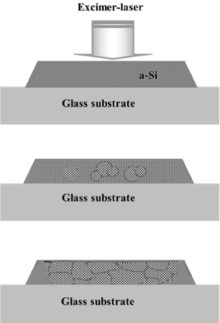
Schematics of nucleation and crystal growth of Si in TFTs during excimer-laser annealing process.
The thermal conductivity of the substrate materials is a key factor in determining the cooling rate of excimer-laser annealed Si because the nucleation and crystallization processes of Si are controlled by the unidirectional heat flow from molten Si to the substrate material. Many researchers have reported that MD simulations can be used to interpret the thermal and structural properties of Si.9) Therefore, the implementation of MD simulation to analyze the thermal conductivity under unidirectional heat flow will be a good technique to obtain the time-averaged atomic quantities and fluctuations that are needed to calculate the thermal properties of Si.
In order to obtain the thermal and structural properties of Si in atomic scale, we employed the natural cooling system introduced by Lee et al.10–15) They applied a combination NVT and NVE ensemble to reproduce the ELA process using MD simulation. Nucleation and crystallization processes of laser annealed Si, which result in heat flow from high energy regions that absorb the laser energy to low energy regions that act as heat sinks, were successfully reported. In the present study, MD simulations have been carried out to understand the thermal properties of c-Si and the effects of the microstructural characteristics of a-Si in the ELA process. The feasibility of performing thermal conductivity computing processes using MD simulations will be discussed.
2. Calculation Details
The most important element of MD simulations is the selection of the potential that describes the interactions among atoms. During calculations, the interatomic forces for Si were calculated using the Tersoff potential. The Tersoff potential consists of the many-body interactions included in the bond order term for Si. This potential has been used to study the lattice dynamics,16) thermo-mechanical properties,17) point defects,18) and the liquid and amorphous phases of Si.19,20) The Tersoff potential describes well the properties of both crystalline and liquid phases of Si.21) Although the Tersoff potential gives rise to a high melting temperature about 2500 K, it describes the thermal and structural properties of solid and liquid Si well.16)
Herein, the thermal conductivity of c-Si was obtained by means of a direct method. Fig. 2 shows the whole modeling procedure used to calculate the thermal conductivity of c-Si. The direct method is a non-equilibrium method that relies on imposing a temperature gradient across the MD cell. Therefore, it is similar to the standard experimental conditions, which involve measuring the stationary heat flux necessary to maintain a temperature gradient. This method is only valid when a stable, linear temperature profile is obtained in the system. In other words, it requires first the establishment of a steady state, and then that heat flow in the direction of the temperature gradient should be uniform. If a linear temperature profile is established, the thermal conductivity can be obtained using Fourier’s law of heat flow J,
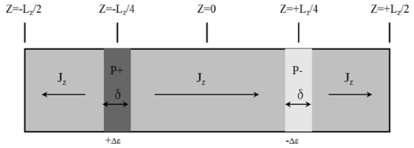
Schematic representation of periodic simulation cell. The cell was divided into slices to determine the thermal conductivity of c-Si. There is a layer of thickness δ at z = −Lz/4 into which energy Δɛ is added; in the layer at z = +Lz/4, energy Δɛ is removed at each MD step.
where Δt is the time step used in the MD simulation, A is the cross section area of the system, and Δɛ is a constant energy that is added to and removed from the heat source and heat sink layer. The thermal conductivity can be expressed as:
Here, ∂T/∂x is the temperature gradient.
During the simulations, a steady-state heat flow was generated for a given sampling time by scaling the velocity of the atoms, which are located in the heat source and the heat sink layer, as shown in Fig. 2. The MD cells, which have a length of a few tens of nm in the direction of the heat flow, were used. The equations of motion were integrated using the velocity Verlet algorithm. All the atoms were placed in their initial positions and provided with initial velocities at 1000 K. We considered the heat source and heat sink layer as having a 2 Å thickness in the direction perpendicular to the heat current, which is located at z = Lz/4 and z = 3Lz/4 in the MD cell of length Lz. At each calculation, the atoms inside the slices were determined and constant energy was added to a thin slice centered at z = Lz/4 (heat source) and the same energy was removed from a layer centered at z = 3Lz/4 (heat sink) by rescaling the particle velocity at each MD time step of 0.5 fs. By imposing the heat in this manner, a constant heat flux per unit area Jz, which is equal to Δɛ / (2L2Δt), was obtained (the factor 2 comes from the fact that the heat flux coming from the hot layer divides equally into two parts to reach the cold layer). When the system achieved a steady state, the appropriate temperature gradient was obtained between the heat source and the heat sink layer. The calculations for the thermal conductivity of c-Si were performed after measuring the temperature gradients.
The structural property of a-Si prepared by natural cooling was investigated using the MD cell with the size of 48.9 × 48.9 × 97.8 Å3. MD simulations were performed under constant NVT conditions (i.e., constant number of particles N, constant volume V, and constant temperature T), using an MD cell with periodic boundary conditions. Periodic boundary conditions were employed in the [100] and [010] directions. The solid-liquid interface was prepared by setting the temperature of the atoms at 300 K and 3500 K for Z ≤ 35 Å and Z > 35 Å of the MD cell, respectively. Temperature was controlled using the ordinary Langevin equations; we employed the scheme developed by Gunsteren and Berendsen for the numerical integration of the Langevin equations. The Langevin equation for the motion of atom i is:
where Fi(t) is the sum of all forces exerted on atom i by other atoms and can be derived from the potential, which is dependent on the coordinates of all N particles. mi is the mass of the atoms, and γ is the friction constant. The time step for the integration was set at 0.002 ps and the friction coefficient was set at 5 ps−1. For the natural cooling processes employed in this study, the combination NVT and NVE ensemble (i.e., constant number of particles N, constant volume V, and constant energy E) was applied. During cooling, only the temperature of the bottom 10 Å of the MD cell was controlled at 300 K. The simulation procedures are described in detail elsewhere.10–13)
3. Results and Discussion
In the case of crystalline materials, heat is carried by phonons, which can influence the transport of heat. Usually, long simulation times are needed to achieve a smooth temperature profile because phonon-phonon scattering events in a solid are far less frequent than particle collisions in a fluid and are amorphous when phonon-phonon scattering is the dominant mechanism for thermal resistance.22) Therefore, the simulation times of the 2 × 10⁶ MD steps with a time step of 0.5 fs were applied to achieve a smooth temperature profile.
As mentioned above, the steady-state heat flow is an important criterion for the reasonability of Fourier’s law when calculating the thermal conductivity. The steady-state heat flow can be measured using a stationary temperature profile as a function of time. Fig. 3 displays the time evolution of the time-averaged temperature at z = 59.9 nm and z = 99.9 nm at 1000 K. At the specific position z, the time-averaged temperature in a thin slice is given by
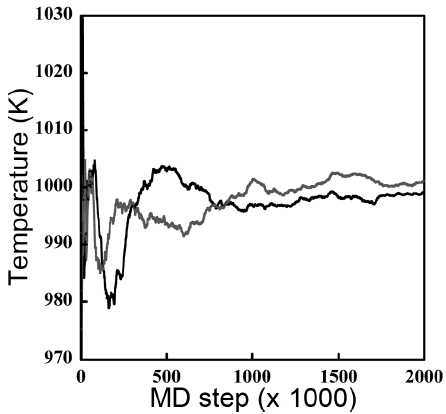
Time evolution of time-averaged temperature for slices at 20 nm away from heat sink. Gray and black curves are the temperatures at Z = 59.9 nm and Z = 99.9 nm for a 4 × 4 × 196 system at 1000 K.
where <T(z)>M is the time-averaged temperature at z, M is the time step, and TN-m(z) is the instantaneous temperature at z for the time step N-m. Here, N is the total number of time steps. To obtain steady-state heat flow, the temperatures in both slices were first averaged over 1000 MD steps to eliminate the large temperature fluctuations. The temperatures at both positions fluctuate significantly for a few ps and stabilize after 150 ps. The steady state was achieved in 1 ns. We found a difference of about 2 K between the two layers.
The temperature gradient was calculated by dividing the MD cell into slices with thickness of 2 Å along the heat flow direction. The average temperature in a thin slice was computed at each MD step. As shown in Fig. 2, the presence of the heat source and heat sink and the application of periodic boundary conditions in all directions generated a heat current in two opposite directions. The thermal conductivity (κ) is calculated by linear fitting of the temperature gradient in the intermediate region of the average temperature profile.
To determine whether Fourier’s law is obeyed, it is essential to check whether the value of κ does in fact depend on the choice of Δɛ. Because the heat current is proportional to Δɛ/A, this is performed by computing for several different energy values from 0.0003 to 0.01 eV. Fig. 4 shows the effect of changing Δɛ for a 4 × 4 × 96 system at 1000 K. Although these results show a bit variation of with Δɛ, the values of κ are not appreciably affected by the changes of Δɛ. No significant deviations from Fourier’s law are apparent in Fig. 4. Extrapolation of the system size Lz to infinity yields an accurate κ of 58 W/mK at 1000 K.
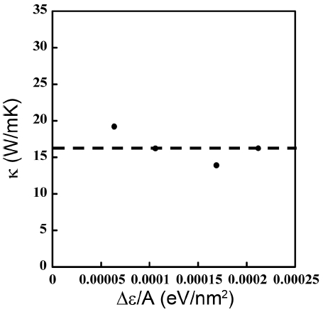
Effect of changing Δɛ for a 9 × 9 × 96 system at 1000 K.
Because the thermal conductivity can be calculated well using MD simulations, we performed a natural cooling computation to prepare a-Si. In this way, the heat is moved from l-Si to the temperature-controlled region. The heat and temperature changes during natural cooling are shown in Fig. 5 and 6. Rapid heat release by heat diffusion from l-Si to the temperature-controlled region is observed and, as a result, the heat flow through c-Si induces a considerable temperature gradient in the l-Si region. A temperature transition layer, with a thickness of about 10 Å at the solid-liquid interface after melting, can be observed in Fig. 6, but this soon disappears during natural cooling. This phenomenon is attributed to the temperature control of 10 Å of c-Si region and the heat flow through the c-Si region, both of which lead to the linear temperature gradient being at the interface, unlike previous results.10–12) Considering the fact that the heat release rate from l-Si into the temperature-controlled regions depends not only on the heat flow within the bulk l-Si but also on the thermal conductivity of c-Si, the relatively rapid cooling rate of ~1013 K/sec can be attributed to the high thermal conductivity of c-Si and the short distance between the heat removal regions and the solid-liquid interface. Because we consider that the MD cell used in this simulation is relatively too small to allow a correct interpretation of the cooling rate, it can be expected that significant improvements will be possible in the future.
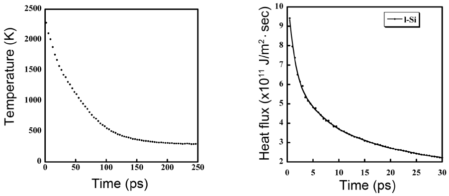
Temperature change (a) and variation of heat flow (b) of system during natural cooling. The temperature of bottom 10 Å of MD cell was set at 300 K.
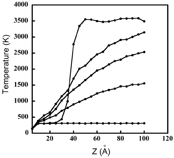
Local temperature changes obtained by mean kinetic energy during natural cooling with time.
For theoretical understanding of the thermal equilibrium during natural cooling, the velocity distribution of atoms (VDA) in the local area was investigated. Fig. 7 shows the changes of VDA in the region of 90 ~ 95 Å at two different times of 160 and 170 fs, respectively, during natural cooling. The dashed lines indicate the VDA obtained theoretically using the Maxwell-Boltzmann function with the averaged local temperatures. The Maxwell-Boltzmann distribution of VDA indicates that the system is in thermal equilibrium during natural cooling. The cooling rate of ~1013 K/sec leads to the formation of a-Si.
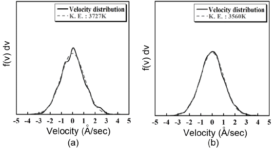
Velocity distribution changes during natural cooling in the region of 90 ~ 95 Å at (a) t = 160 fs and (b) t = 170 fs, respectively.
In order to determine the dynamical properties of naturally cooled a-Si, the static structure factors S(k) are calculated by Fourier transforming of the pair-correlation functions g(r),10)
Here, ρ0 is the average number density of atoms and k is the wave number of the diffracted wave. The atoms lying over 50 Å of the MD cell were sampled to investigate the structural properties. It should be noted that the setting temperature for preparing l-Si is about 3500 K, with a density of 2.33 g/cm3. The k < 1.5 Å−1 region contains truncation error and should be ignored. In the case of l-Si, it can be clearly seen that the first peak is asymmetric. This shows the existence of some covalent bonds and the reminiscent of the crystalline characteristics in the liquid.23) The peak shape resembles that of S(k) for a supercooled metallic liquid Si.24) This result supports the metallic behavior of the melt, as expected. With decreasing temperature, the first peak splits into two and these two peaks develop and appear at low temperature. The appearance of a new shoulder of the third peak is in good agreement with the experimental results.25) This spectrum of the peak indicates the short-range order of a-Si.
4. Conclusions
MD simulations have been performed to calculate the thermal conductivity of c-Si via the direct method. Calculation procedures for thermal conductivity were proposed and reliable results were obtained using Fourier’s law at 1000 K. The results for the steady-state heat flow and the effect of changing Δɛ confirmed that Fourier’s law was satisfied during the thermal conductivity calculation of c-Si. To prepare a-Si, natural cooling simulation was performed with a combination NVT and NVE ensemble. A temperature transition layer was observed at the interface after melting faded away during natural cooling, and a linear temperature gradient was found at the interface instead. The static structure of a-Si quenched with a cooling rate of ~1013 K/sec showed the appearance of a new shoulder on the third peak, suggesting that a-Si generated by natural cooling described the characteristic of experimentally prepared a-Si well. MD simulations using a large system, which could be compared with the film thickness used in the ELA process, are under study.
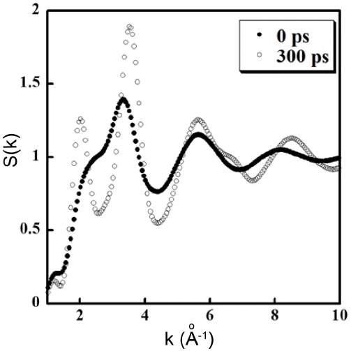
Static structure factors S(k) of Si. Closed and open circles denote the static structure factors of a-Si naturally cooled at 300 K and l-Si prepared at 3500 K, respectively.