Properties of Working Electrodes with IGZO layers in a Dye Sensitized Solar Cell
Article information
Abstract
We prepared a working electrode (WE) coated with 0 ~ 50 nm-thick indium gallium zinc oxide(IGZO) by using RF sputtering to improve the energy conversion efficiency (ECE) of a dye sensitized solar cell (DSSC). Transmission electron microscope (TEM) and energy dispersive spectroscopy (EDS) were used to analyze the microstructure and composition of the IGZO layer. UV-VIS-NIR spectroscopy was used to determine the transparency of the WE with IGZO layers. A solar simulator and a potentiostat were used to confirm the photovoltaic properties of the DSSC with IGZO layer. From the results of the microstructural analysis, we were able to confirm the successful deposition of an amorphous IGZO layer with the expected thickness and composition. From the UV-VIS-NIR analysis, we were able to verify that the transparency decreased when the thickness of IGZO increased, while the transparency was over 90% for all thicknesses. The photovoltaic results show that the ECE became 4.30% with the IGZO layer compared to 3.93% without the IGZO layer. As the results show that electron mobility increased when an IGZO layer was coated on the TiO2 layer, it is confirmed that the ECE of a DSSC can be enhanced by employing an appropriate thickness of IGZO on the TiO2 layer.
1. Introduction
Dye sensitized solar cell (DSSC) is a solar cell using the principle of photosynthesis, and was first reported by professor Michael Grätzel of chemistry department at Swiss Federal Institute of Technology in Lausanne in 1991.1) DSSC has a very low price at about 20 ~ 30% of the price for the existing silicon solar cells due to simple manufacturing processes compared with the latter. However, the energy conversion efficiency (ECE) of DSSC remains in a standstill condition at about 11% which is a half of the level for silicon solar cells.2) For improving this problem, active studies of DSSCs are currently being conducted.
DSSC consists of a counter electrode (CE), an electrolyte, and a working electrode (WE). The CE is composed of transparent conductive oxide (TCO) substrate and a catalyst layer. Since the CE plays a role of transferring the electrons having moved through an external circuit to the electrolyte, the catalyst material should have a high electrical catalyst activity and a high conductivity.3) Although platinum (Pt) was mainly used in the case of existing catalyst materials, application studies of diversified materials with economy and thermal stability to substitute for the expensive Pt have been reported.4,5)
For the electrolyte which plays a role of oxidation-reduction the electrons moved through the CE, there are iodide mixture, iodine dissolved in a nonprotonic solvent, LiI,6) NaI,7) acetonitrile, and propionitrile,8) etc.
Also, the WE consists of TCO substrate and semiconductor oxide of TiO2, and dye coated on the TiO2 particles, where the TCO substrate includes indium tin oxide (ITO), fluorine doped tin oxide (FTO), aluminum doped zinc oxide (AZO), etc., and the FTO is used most frequently among them because of its excellent thermal stability, relatively low surface resistance and a high transmissivity exceeding 80%.9) The dye plays a role of generating an electromotive force for DSSC by producing holes and electrons upon incidence of light, the types of which include Ru-based organic metal compounds, organic compounds, and proton inorganic compounds such as N3, N719, N749, etc. Meanwhile, the semiconductor oxide is an important element with many effects on the change in energy conversion efficiencies for DSSC, since it transfers the electrons produced by dye molecules to the TCO substrate. Types of the semiconductor oxide as a layer for transferring the electrons produced by opto-electronic effects include TiO2, ZnO, SnO2, Al2O3, etc., and many studies to improve electron mobility and prevent electron recombination are in progress for improvement of efficiencies of DSSC through combination of different semiconductor oxides by using band gap differences for each oxide semiconductor. S. Chappel et al.10) have reported that electron mobilities were improved and short circuit current densities were increased from at least 5.7 mA/cm2 to 6.4 mA/cm2 by reducing the band gap difference between the dye and SnO2 through coating of TiO2 onto SnO2 particles. E. Palomares et al.11) have reported that the efficiency was increased from the existing 3.8% to 5.0% by reducing electron recombination through coating of Al2O3 with a relatively large band gap of 7.0 eV onto TiO2 with a band gap of 3.2 eV. Also, S. G. Chen et al.12) have reported the efficiency of 5.0% improved by 35% in comparison with the existing efficiency of 3.6% by improvement of electron mobilities through coating of a thin Nb2O5 layer onto the TiO2 layer. However, engineering using such semiconductor oxides has a limitation in increasing the electron mobilities for electron transfer resulting in a limitation in improvement of DSSC efficiencies through this method. Therefore, improvement of electron mobilities is required in reality through combination of materials with a high electron mobility unlike the existing semiconductor oxides.
Indium gallium zinc oxide (IGZO) is a compound composed of indium (In), gallium (Ga), zinc (Zn), and oxygen (O), and one of transparent amorphous oxide semiconductors. IGZO has uniform characteristics of an amorphous substance and a high electron mobility of about 1 ~ 100 cm2/Vs, so that it has been employed as a thin film transistor for large-screen, high-speed, high-quality flat panel displays.13) IGZO shows a high electron mobility without a large variation with processes or heat treatment conditions despite being amorphous, and has excellent characteristics in comparison with many other amorphous materials exhibiting a low-level mobility.14)
Also, such IGZO is expected capable of providing help to efficiency improvement for DSSC by decreasing electron losses through reduction of electron recombination since it has not only characteristics of inherently high electron mobility but also a smaller band gap of 3.0 eV than that of TiO2 (3.2 eV).
In this study, we coated IGZO with thicknesses of 0 ~ 50 nm on TiO2 layers in DSSC to improving ECE with an excellent electron mobility.
2. Experimental Procedure
In this study on DSSCs, we prepared the TiO2 coated IGZO with a thickness of 0 ~ 50 nm.
We made 300 nm-thick blocking layers (BLs) by mixing titanium(IV)bis(ethyl aceto acetato)-diisopropoxide and 1-butanol into a solution, followed by spin-coating for 500 rpm-10 sec. and 2000 rpm-40 sec., and heat treating at 500°C for 15 min. We fabricated the 8 μm-thick TiO2 films by coating TiO2 paste (Dyesol DSL 18NR-T of 10) via doctor blade method, and by heat treatment at 500°C for 30 min.
After coating of TiO2 layer, IGZO thin films with a thickness of 10, 30, and 50 nm were coated onto TiO2 films by using a RF sputter (PSP5004, SNTEK). At this time, the process was implemented by using a 4-inch IGZO target while rotating the substrate at 5 RPM with the distance between target and substrate of 100 mm. The base pressure was less than 3.0 × 10⁻⁶ torr, and Ar gas was introduced by 20 sccm at room temperature. Here, the IGZO alloy target was produced for a composition of In : Ga : Zn = 1 : 1 : 1.
To check for microstructures, vertical section specimens were prepared by using a focus ion beam (FIB, NB 5000, Hitachi) with Au, W layers being coated onto the upper part of IGZO as a protection layer for transmission electron microscopy (TEM) analysis. With utilization of TEM (HF-3300, Hitachi) equipment, cross section structures of IGZO were checked in a dark field mode, and crystallinity of the IGZO layer was checked through nano beam electron diffraction (NBED) analysis. At this time, observation was carried out under the conditions of 5 nm in beam size, 30 cm in camera length, and 0.00197 nm in wave length.
To check for compositions of IGZO film, energy dispersive spectroscopy (EDS, JSM-6010LA, JEOL) was used. After magnification to 100 times using an acceleration voltage of 15 kV, contents of each constituent element were quantitatively analyzed.
Transmittance of the prepared WE was analyzed by UV-VIS-NIR (UV3105PC, Shimadzu) with an transmittance-mode apparatus under medium scan speed. At this time, measurement of transmittance for IGZO layers in each sample was completed by setting the WE with a structure of glass/FTO/BL/TiO2 for the 100% reference point. Average transmittance in the visible-light region of 400 ~ 800 nm was obtained by adding absorbances at each wavelength and dividing it by the number of added times.
Lastly, the WE with a structure of glass/FTO/BL/TiO2/0 ~ 50 nm IGZO/dye (N719) was completed as shown in the bottom part of Fig. 1 by adsorption of 0.5 mM cis-vis bis-ruthenium (II) bis-tetrabutylammonium (N719).
The CE was prepared by RF sputter (MHS-1500, Moohan, 300 W, 13.56 MHz) to form a 100 nm-Pt film on a glass substrate using 99.99% Pt as a target. A flow of 40 sccm Ar at pressure of 5 mtorr at RT was set for the process. The prepared WE and CE were fixed at position and filled with electrolyte, finalizing DSSC device consisted glass/FTO/BL/TiO2/IGZO/dye (N719)/electrolyte/100 nm Pt/glass with active area of 0.45 cm2 as shown in Fig. 1.
To check for interface resistance of the completed devices, impedances were measured by using a solar simulator (PEC-L11, Peccell) and a potentiostat (Iviumstat, Ivium). Internal impedances were analyzed by measuring the results of current response to application of each AC voltage in the frequency range of 10 mHz ~ 1 MHz.
I-V (current-voltage) characteristic of DSSC was measured by the same instruments under a setup; a 100 W Xenon lamp was the illumination source at 1 sun (100 mW/cm2) condition. For I-V analysis, short circuit current density (Jsc), open circuit voltage (Voc), fill factor (FF), and energy conversion efficiency (ECE) were checked together.
3. Results and Discussion
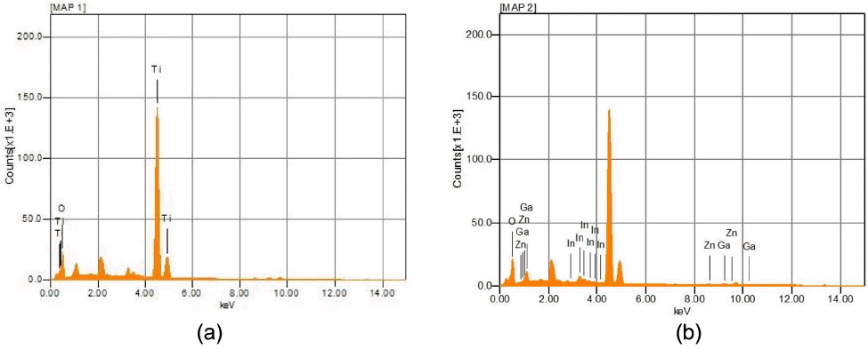
Figure 2 shows EDS analysis results for the WE with (a) 0 nm and (b) 50 nm of IGZO. Fig. 2(a) represents the result of checking for composition of the WE (glass/FTO/BL/TiO2) without coating of IGZO where characteristic peaks of Ti and O were observed and appeared in the ratio of about 1:2, allowing confirmation that TiO2 was formed as intended.
Figure 2(b) represents the result of checking for composition of the WE (glass/FTO/BL/TiO2/IGZO) coated with 50 nm of IGZO, and analysis was conducted after removal of Ti peaks to remove the effects of the lower TiO2 layer. Respective peaks of In, Ga, Zn and O as an element of IGZO were confirmed, and the ratio for In, Ga, Zn was measured to be about 1 : 1 : 0.4 upon relative calculation with O excluded. Meanwhile, the contents of O were shown to be high, as the O contained in the TiO2 layer coated on the lower part was measured together. Although the IGZO layer was confirmed to be a thin film with a slightly low content of Zn as compared with the target produced for the composition of In : Ga : Zn = 1 : 1 : 1, the intended IGZO layer could be ultimately confirmed to have been deposited.
Figure 3 shows TEM images magnified to 50,000 times for the WE having a structure of glass/BL/TiO2/IGZO with (a) 10 nm, (b) 50 nm of IGZO. The image inserted in the upper left corner represents the result of NBED analysis for IGZO thin film.
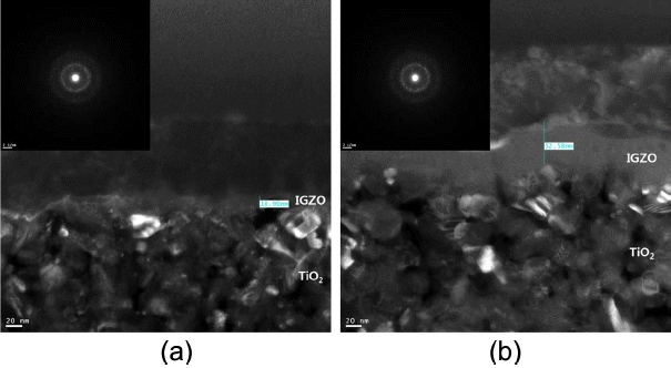
TEM data for IGZO of (a) 10 nm and (b) 50 nm in thickness. Insets are nano beam electron diffraction images.
Fugure 3(a) shows a TEM analysis image for the WE coated with 10 nm of IGZO, allowing confirmation of existence of TiO2 having a particle size of about 20 nm. In the case of IGZO layer, a relatively bright color could be observed as compared with TiO2 layer, and coating to a thickness of about 10 nm could be confirmed. Also, the IGZO thin film could be confirmed to be not so uniformly coated onto the lower TiO2 layer, which was considered to be the phenomenon appearing due to coating onto the TiO2 layer with a relatively high surface roughness as the coating result using a PVD method of sputtering. Meanwhile, considering the NBED image for the IGZO thin film inserted in the upper left corner, amorphous IGZO thin films could be confirmed to have been coated on the basis of the fact that the characteristic peaks were not visible.
Fugure 3(b) shows a TEM analysis image for the WE coated with 50 nm of IGZO. In the same manner as with (a), TiO2 layer and IGZO layer could be confirmed, and about 50 nm-thick IGZO thin film could be seen to have been uniformly coated onto the lower TiO2 layer unlike with (a). Also, considering the NBED image for the IGZO thin film inserted in the upper left corner, the characteristic peaks were not visible in the same manner as with (a), amorphous IGZO thin films could be confirmed to have been coated.
Therefore, successful coating of amorphous IGZO thin films to the intented thickness could be hereby confirmed.
Figure 4 shows the transmittance results for glass/FTO/TiO2/IGZO with deposition of IGZO. The analysis results for transmittance within the visible light domain in wavelength range of 400 ~ 800 nm are shown for each WE with deposition of 0, 10, 30 and 50 nm of IGZO. Average transmittances in the case of deposition of 10, 30, and 50 nm of IGZO were measured to be 95.46, 95.59, and 91.71%, respectively, while transmittance for the sample with 0 nm of IGZO was 99.00%, confirming that the transmittance was gradually reduced in comparison with the sample without deposition of IGZO. However, transmittance of the visible light upon coating of IGZO was higher than 90% in all cases, confirming that there was no large difference in comparison with the device without deposition of IGZO.
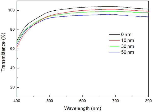
Transmittance data in visible light region for TiO2 layers with IGZO having thicknesses of 0 ~ 50 nm.
Therefore, even with employment of IGZO, transmittance as an electrode body for the DSSC device was shown to be excellent, suggesting that the thickness of IGZO would not have a great effect on the energy conversion efficiency of DSSC.
Figure 5 shows Nyquist diagrams consisting of a real number term and an imaginary number term for the frequencies applied to a DSSC device with deposition of 0 ~ 50 nm of IGZO along with an equivalent circuit.

(a) Impedance spectra of the DSSCs employing IGZO of 0 ~ 50 nm in thickness, and (b) equivalent circuit model.
Fugure 5(a) shows Nyquist diagrams for the DSSC device with deposition of 0 ~ 50 nm of IGZO, confirming appearance of 3 types of semi-circles (R1, R2, R3) as in the general internal resistance of DSSC. R1 value is the interface resistance related to the resistance of FTO/TiO2 interface and the resistance to electric charge movement of electrolyte/CE interface at 103–105 Hz, and was about 1.5 Ω showing similar values within the error range upon deposition of 0 ~ 50 nm IGZO by using the same electrolyte and CE in this study. Also, R2 value is related to the resistance to electron movement in TiO2 and the interface resistance of TiO2/electrolyte interface at 1–103 Hz. Whereas the value of 9.8 Ω is observed for the device without deposition of IGZO, it was reduced to 9.0 Ω in the case of a device with deposition of 10 nm of IGZO, but could be seen to be increased again to the values of 10.8 and 10.7 Ω as the thickness was increased to 30 and 50 nm, respectively. This was considered to be the phenomenon where the interface resistance between TiO2 and electrolyte was increased so as to increase R2 value again when the thickness of IGZO layer was increased to more than a given value although the resistance to electron movement was reduced so as to decrease R2 value upon coating of IGZO with a high electron mobility onto TiO2 layer.
Fugure 5(b) shows an equivalent circuit displayed considering the case with coating of IGZO onto TiO2 layer, where RTiO2 represents the resistance of TiO2 with RIGZO(I) and RIGZO(II) representing a resistance of IGZO. At this time, RIGZO(I) and RIGZO(II) may be given by the equation (1) and the equation (2), respectively, where k is the constant, μ the electron mobility, R the resistance, and t the thickness of thin film. Since RIGZO(II) value can be neglected as the IGZO thin film becomes thinner, convergence to RIGZO(I) value may be confirmed. On the other hand, it can be confirmed that RIGZO(II) values are increased accompanied by an increase in the overall resistance as the IGZO thin film becomes thicker. Meanwhile, R3 value corresponds to the Warburg impedance related to diffusion of oxidation-reduction species in the electrolyte at higher frequencies than 106 Hz, was shown to be a similar value of about 2.7 Ω, due to the use of the same electrolyte.
Consequently, when an appropriate thickness of IGZO was employed for TiO2 layer, electron mobilities were increased which was considered capable of helping for an increase in DSSC efficiencies.
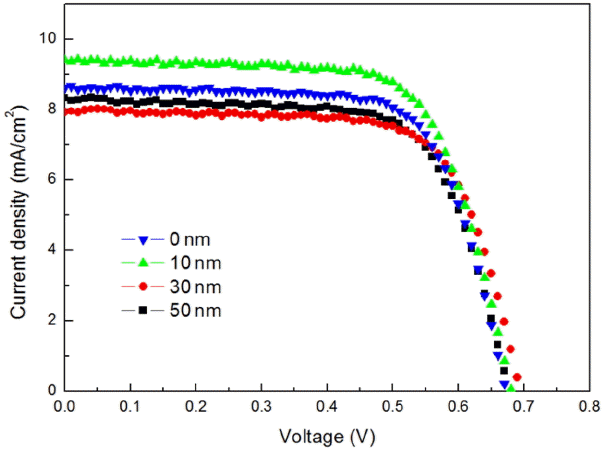
Figure 6 shows I-V data for measurement of opto-electronic conversion efficiencies of the DSSC devices having a structure of glass/FTO/BL/TiO2/IGZO/dye (N719)/electrolyte/100 nm Pt/glass which employed 0 ~ 50 nm of IGZO. In the case of the device without coating of IGZO as compared with the device with 10 nm of IGZO coated, short circuit current densities could be confirmed to be low, and were shown to be reduced as the thickness of IGZO was increased. FF was an element related to interfacial resistance of the entire DSSC device, and confirmed to be reduced with coating IGZO.
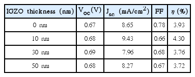
Table 1 is a summary of results for I-V curves of Fig. 6. Upon deposition of 0, 10, 30, and 50 nm IGZO, Voc were shown to be 0.67, 0.68, 0.69 and 0.68 V, respectively, allowing confirmation that similar values within the error range were observed. It is considered that the Voc as an element related to oxidation-reduction reaction of the electrolyte were measured to be the same since the same electrolyte was used in all of the present experiments.
In the case of Jsc, a value of 8.65 mA/cm2 was observed for the device without employing IGZO, while it was confirmed to be relatively increased to 9.43 mA/cm2 upon employment of 10nm of IGZO. This was a result of employing the IGZO with a high electron mobility, and was in agreement with the previous impedance result of reduction in R2 values. Meanwhile, in the case of employing 30 and 50 nm of IGZO, the Jsc could be confirmed to be reduced again to 7.96 and 8.27 mA/cm2, respectively. This was considered to be the result of an increase in interface resistance with thick coating of IGZO layer between TiO2 layer and electrolyte in a similar way to the previous impedance result.
In the case of FF as an element affected by interface resistance, it was observed to be reduced to 0.66, 0.68 and 0.67 upon deposition of 10, 30 and 50 nm of IGZO, respectively, whereas it was shown to have a value of 0.78 for the device without deposition of IGZO. This was considered to be the result attributable to an increase in sheet resistance for the entire device as the amorphous IGZO was employed.
Consequently, final efficiencies were confirmed to be reduced again due to an increase in interface resistance upon thickening to more than 30 nm, while they were increased up to 10 nm according to a change in short circuit current densities. When an appropriate thickness of IGZO was employed, ECE for a DSSC device could be improved due to improvement in the electron mobilities.
4. Conclusions
0 ~ 50 nm of IGZO was employed for TiO2 layer of the WE in a DSSC, and the corresponding changes in material properties and opto-electronic characteristics of the DSSC were confirmed. According to the results of microstructure, successful coating of IGZO was realized and UV-VIS-NIR results, excellent transparencies higher than 90% were observed, although the transparency was reduced as the thickness of IGZO was increased. While final energy conversion efficiencies of DSSC devices were increased due to an increased electron mobility compared with the existing case when 10 nm of IGZO was employed, they eventually exhibited the phenomenon of being reduced due to the continued increase in its own resistance when the thickness of IGZO layer was increased. Consequently, ECE of a DSSC device could be increased by employing an appropriate thickness of IGZO for TiO2 layer.

