


1. Introduction
In today’s complex information society, the importance of the reliability of electronic components and electrical and electronic equipment must be emphasized more than ever. A reliable system maintains stability under complex circumstances; the system should be not disturbed from external circumstances, in particular, transient and overvoltage. However, a semiconductor circuit system is very sensitive to overvoltage. As a result, devices or systems can malfunction or be destroyed by overvoltage. Therefore, surge protection devices (SPDs) must be embedded into systems. The core element of an SPD is a varistor.
A varistor is a semiconductor device, in which the current nonlinearly varies with voltage.1) If the nonlinear coefficient, which shows the degree of nonlinearity, is high, it can define the varistor as follows. The varistor will play a role as an insulator at a lower voltage than the breakdown voltage, and a conductor at a higher voltage than the breakdown voltage.
Most reported varistor materials have been Bi-doped zinc oxide1-7) and Pr-doped zinc oxide.8-10) These materials need high sintering temperatures of more than 1000°C. An internal electrode to fabricate a multilayered varistor is necessarily needed. Thus, in general, the internal electrode is formed using expensive Pt or Pd. Alternative varistor materials are vanadium-added zinc oxide varistor ceramics.11,12) These have a lower sintering temperature using the low melting point (690°C) of vanadium oxide (V2O5). The history of so-called ZnO-V2O5-based varistor ceramics is much shorter than that of zinc-bismuth-based and zinc-praseodymium-based ceramics. Nevertheless, the technology is advanced using existing varistor technology.
Until now, nonlinearity has been considerably improved whereas stability has not.13-15) A complex process using diverse additives and sintering processes should be continuously conducted to enhance varistor characteristics. The ceramic composition used in this study was selected on the basis of its nonlinear properties, microstructure, stability, etc.13-19) We introduce a V2O5-Mn3O4-Co3O4-Dy2O3-Nb2O5-Bi2O3 (VMCDNB)-doped zinc oxide varistor ceramic exhibiting a relatively high stability.
2. Experimental Procedure
2.1. Sample preparation process
Analytic grade powder materials for the varistor, i.e. 98.25 mol% ZnO + 0.5 mol% V2O5 + 0.5 mol% Mn3O4 + 0.5 mol% Co3O4 + 0.1 mol% Dy2O3 + 0.1 mol% Nb2O5 + 0.05 mol% Bi2O3, were prepared. The varistor devices were created using the traditional ceramics method. The balanced raw materials were ball milled for 24 h with acetone in a polypropylene bottle. The mixture was dried at 120°C in a dry oven. The mixture was blended with polyvinyl butyral (PVB) and granulated using a sieve shaker to obtain a starting powder. The granulated powder was pressed into pellets (approximately 10 mm in diameter and approximately 1.5 mm in thickness) by uniaxial pressing (1000 kg/cm2). The pellets, set on a stabilized MgO plate after burning out the polyvinyl butyral (PVB) binder at 600°C for 1 h, were sintered at various temperatures, i.e. 850, 875, 900, and 925°C, for 3 h. The sintered pellets were lapped and polished into a specified dimension (approximately 8 mm in diameter and approximately 1.0 mm in thickness). The final pellets were coated with conductive Ag paste and then fired at 550°C for 10 min.
2.2. Microstructure examination
The sintered pellets were lapped and polished, and then were etched using 1HClO4:1000 H2O solution (v/v). A fracture microstructure image of the sintered pellets was obtained using field emission scanning electron microscopy (SEM; Quanta 200). The average grain size (d) was calculated using the following expression proposed by Wurst et al.20):
where L is the random line length on the micrograph, M is the magnification of the micrograph, and N is the number of the grain boundaries intercepted by the lines.
The X-ray diffraction patterns of the sintered pellets were obtained using CuKα radiation (X'pert-PRO MPD). The densities (ρ) of the sintered pellets were obtained using a density determination kit (238490) attached to a balance (AG 245).
2.3. J-E characteristics measurement
The current-voltage (I-V) characteristic data were automatically measured by voltage sourcing and current measuring using a source/measure unit (SMU; Keithley 237). The varistor voltage (V1 mA/cm2) was obtained at 1.0 mA/cm2 in the current density. The leakage current (IL) was obtained at 0.8 times the V1 mA/cm2. The breakdown field (E1 mA/cm2), the nonlinear coefficient (α),1) and the leakage current density (JL) were calculated using the following expressions:
where t is the thickness of the specimen (1 mm) and A is the area of the electrode.
2.4. C-V characteristics measurement
The capacitance-voltage (C-V) characteristics were measured using a precision (LCR) meter (QuadTech 7600) and an electrometer (Keithley 617). The donor concentration Nd and the barrier height Φb were determined using the following expression:21)
where Cb is the capacitance per unit area of a grain boundary, Cbo is the value of Cb when Vg = 0, Vg is the applied voltage per grain boundary, q is the electronic charge, and e is the permittivity of ZnO (ɛ = 8.5ɛo).
The density of the interface state Nt at the grain boundary was calculated using the following expression:21)
2.5. Degradation characteristics measurement
The degradation characteristics were measured under stress such as 0.85 E1 mA/cm2/85°C/24 h. The leakage current (IL) flowing through the varistor was measured every 1 min during the stress by voltage sourcing and current measuring using an SMU (Keithley 237). The degradation rate coefficient (KT) was calculated using the following expression: 22)
where ILo is IL at t = 0.
3. Results and Discussion
Figure 1 illustrates the SEM micrographs of the specimens at various sintering temperatures. On the whole, the grain size of the sintered pellets increased with the increase in sintering temperature. The average grain size (d) of the specimens significantly increased from 4.6 to 8.7 mm, despite the various sintering temperatures of the narrow gap. However, the density (ρ) of the sintered pellets decreased from 5.53 to 5.40 g/cm3 (theoretical density = 5.78 g/cm3 in zinc oxide) with the increase in sintering temperature. It is presumed that the reduction in the density of the sintered pellets can be ascribed to the result of the volatility of ZnV2O4 (see Fig. 2 in advance). The detailed average grain size and density of the sintered pellets at various sintering temperatures are presented in Table 1.
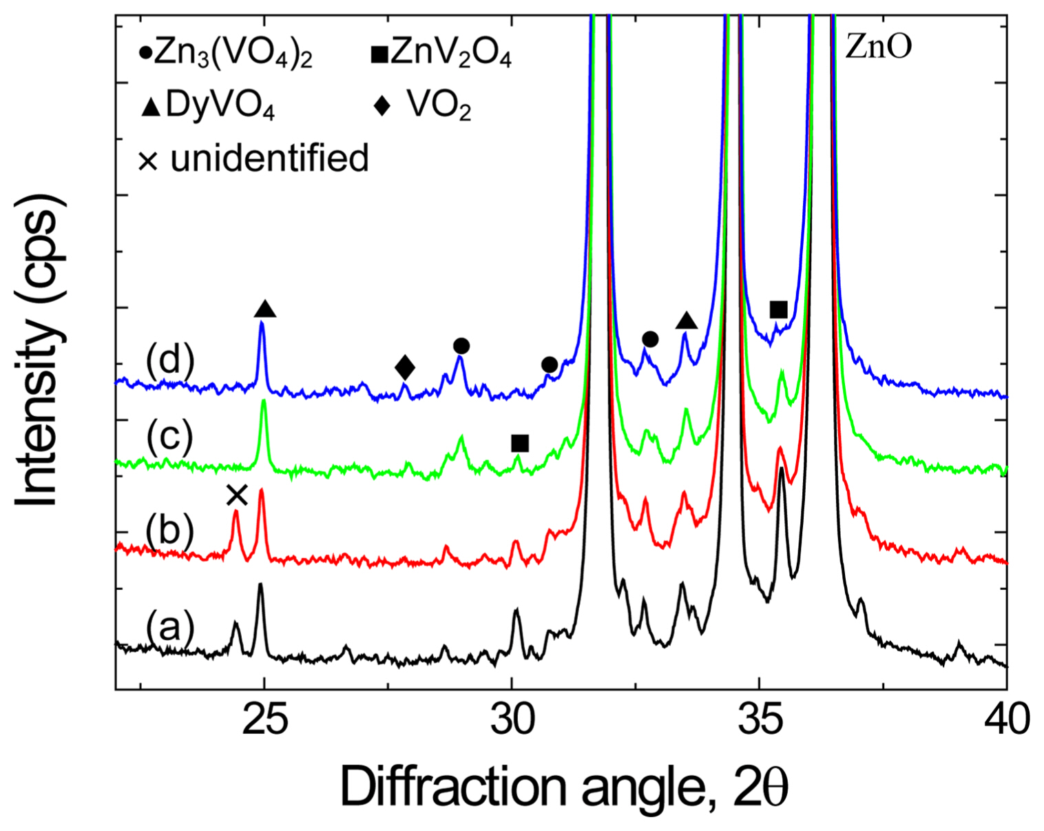
Figure 2 illustrates the X-ray diffraction patterns of the specimens at various sintering temperatures. Minor phases such as the zinc vanadate oxides (Zn3(VO4)2, ZnV2O4), vanadium oxide (VO2), and dysprosium vanadate (DyVO4) were generated. The peak of ZnV2O4 gradually diminished with the increase in sintering temperature. ZnV2O4 most likely volatilizes with of the increase in sintering temperature, despite the various sintering temperatures of the narrow gap. Therefore, ZnV2O4 can affect the sintered density, electrical properties, and stability. In contrast, DyVO4 seems to be considerably stable by indicating the same peak with the increase in sintering temperature.
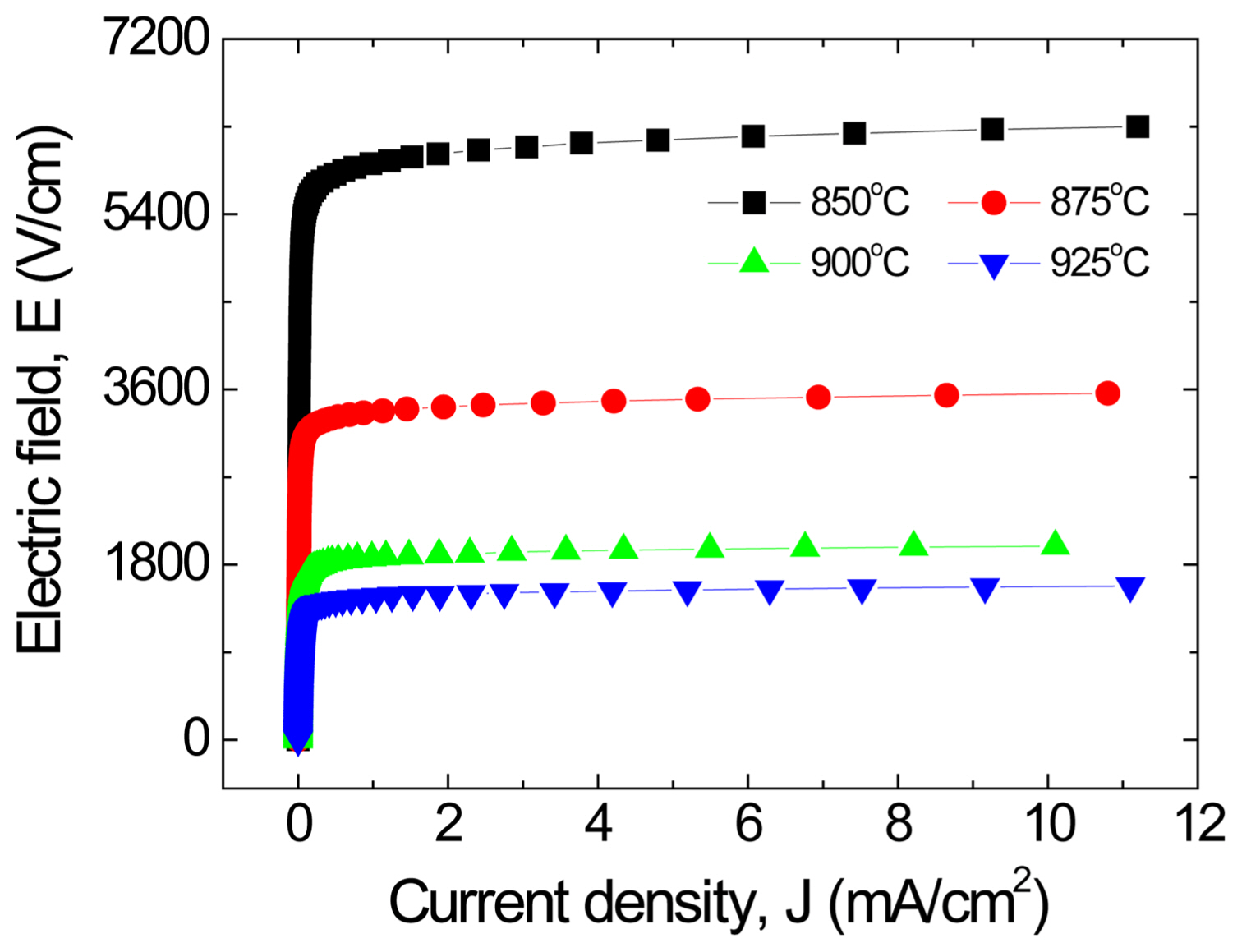
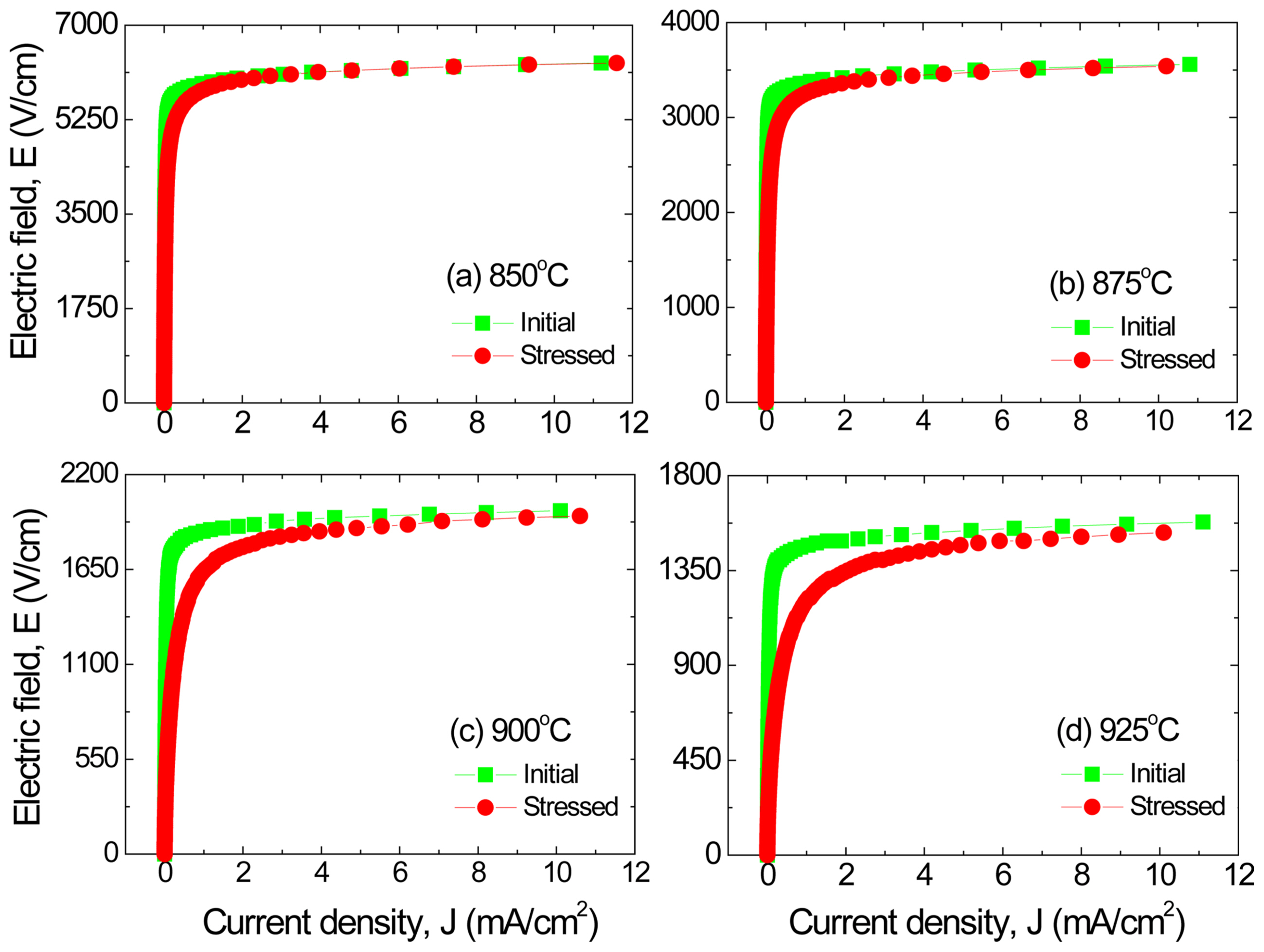
Figure 3 illustrates the electric field-current density (E-J) characteristics of the specimens at various sintering temperatures. The non-ohmicity results from the varistor affect in E-J characteristics. That is, the E-J characteristics are nonlinear in the first and third quadrants. Specifically, the current is nearly zero before reaching a breakdown, and it is almost infinite after reaching a breakdown. The breakdown field (E1 mA/cm2) significantly decreased from 5919 to 1465 V/cm with the increase in sintering temperature. The changing tendency of E1 mA/cm2 was analyzed using the following expression:
where νgb is the breakdown voltage per grain boundary and d is the average grain size. E1 mA/cm2 is directly determined by the d and νgb values. Among them, the average grain size absolutely affects the E1 mA/cm2. Therefore, the reduction in E1 mA/cm2 can be ascribed to the increase in the average grain size with the increase in sintering temperature.
The nonlinear coefficient (α) increased from 39.1 to 43.6 when the sintering temperature reached 875°C. When the sintering temperature exceeded 875°C, α showed a decreasing tendency and diminished to 33.3 at 925°C. In the low field below the breakdown field, the current is dominated by a thermionic emission mechanism, in which the electron is over the potential barrier. In the high field above the breakdown field, the current is dominated by a quantum mechanical tunneling mechanism, in which the electron is through the potential barrier. α is determined by the ratio of the tunneling to the thermionic emission. If the tunneling mechanism is much more predominant than the thermionic emission mechanism, a high α is obtained. Therefore, the higher the barrier, the higher the α. However, the leakage current density (JL) decreased from 35.7 to 28.2 μA/cm2 when the sintering temperature reached 875°C. When the sintering temperature exceeded 875°C, JL increased to 74.1 μA/cm2 at 925°C. The JL value of the specimen sintered at 875°C is a low value comparable to that of ZnO-V2O5-based varistors, which have showed the lowest value until now.14) On the whole, the low leakage current is the important feature of this system. The detailed values of E1 mA/cm2, α, and JL are presented in Table 1.
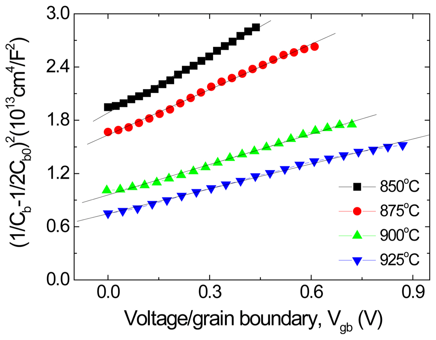
Figure 4 shows the modified C-V characteristics of the specimens at various sintering temperatures. Most of the applied voltage is dropped to the depletion layer width at the grain boundaries. The variation in the space charge within the depletion layer varies the capacitance. Therefore, the donor density (Nd), barrier height (Φb), and density of the interface states (Nt) can be obtained through the variation in the capacitance. Nd is obtained from the slope of the curves. As a result, Nd showed a fluctuation between 0.77×1017 cm−3 and 1.77×1017 cm−3. However, on the whole, Nd seems to increase with the increase in sintering temperature. Φb increased from 0.87 to 0.96 eV when the sintering temperature reached 875°C. When the sintering temperature exceeded 875°C, Φb diminished to 0.80 eV at 925°C. The changing tendency of Φb is equal to that of the nonlinear coefficient. Therefore, the nonlinear properties depend on the potential barrier in the C-V characteristics.
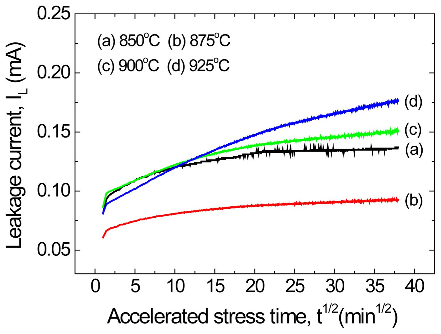
Figure 5 shows the trend of the leakage current (IL) when the specimens are subjected to direct current (DC) stress (0.85 E1 mA/cm2/85°C/24 h). The changing tendency in the leakage current (IL) showed a positive creep phenomenon in which the leakage current increases with increasing stress time for all specimens. The degradation was estimated by the slope KT of the t1/2−IL curves. KT increased with the increase in sintering temperature. The initial leakage current of the specimen sintered at 875°C was the lowest, whereas the KT value (1.38 μA·h−1/2) of the specimen sintered at 850°C was the lowest. In light of the KT value, the specimen sintered at 850°C seems to be the most stable.
Figure 6 illustrates the changing tendency of the E-J characteristic curves after stress, when compared to the initial curves of the specimens at various sintering temperatures. Comparing the initial and stressed curves, the difference, in common, is shown in the vicinity of the knee. The variation is gradually greater with the increase in sintering temperature. The changing tendency of the curves coincides with that of KT. The specimen sintered at 850°C has the highest stability and the specimen sintered at 925°C has the lowest stability.
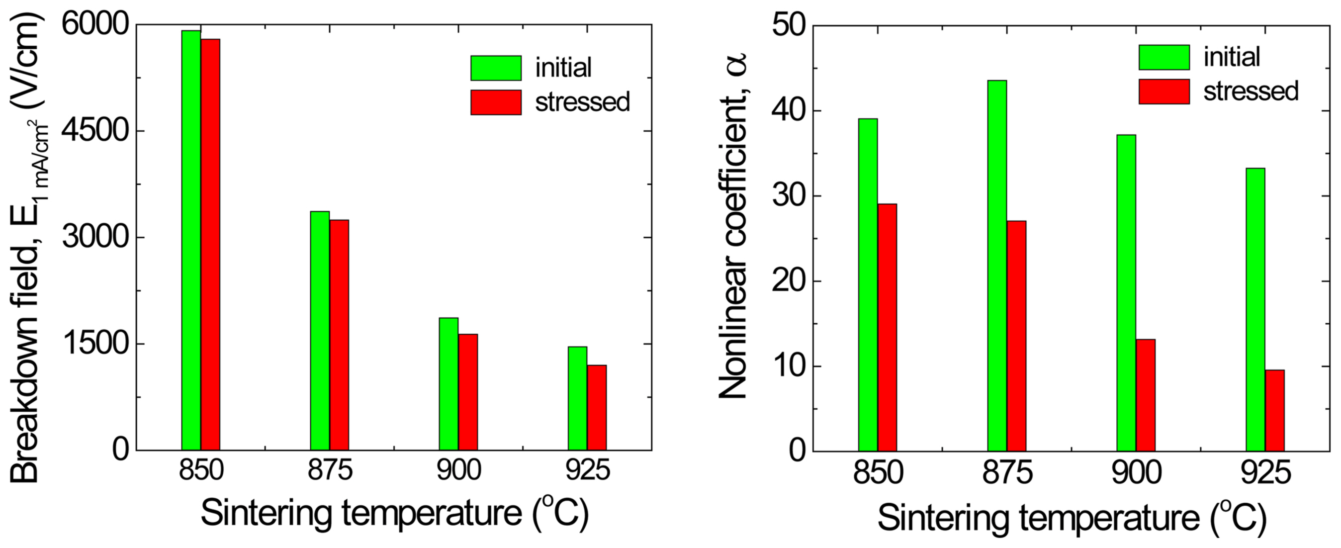
Figure 7 shows E1 mA/cm2 and α of the stressed specimens at various sintering temperatures. Apparently, all the specimens showed a reduction in E1 mA/cm2 after a stress. However, the amount of the reduction differed for each specimen, and gradually increased with the increase in sintering temperature. The specimen sintered at 850°C showed the lowest reduction rate of E1 mA/cm2 with ΔE1 mA/cm2/E1 mA/cm2 = − 2%. However, the specimens exceeding 900°C in sintering temperature showed a large reduction rate, reaching ΔE1 mA/cm2/E1 mA/cm2 > − 10%. Meanwhile, the variation rate of α also had the same changing tendency as that of E1 mA/cm2 with the increase in sintering temperature. However, the reduction rate of α was much larger than that of E1 mA/cm2. The specimen sintered at 850°C showed the lowest reduction rate of E1 mA/cm2 with Δα/α = − 23.3%. a showed the highest value, reaching α = 30 after application of a stress. However, the JL value after a stress increased 4-6 times, when compared to the initial value, unlike E1 mA/cm2 and α. This is a considerable amount. The variation rates of the breakdown field (ΔE1 mA/cm2/E1 mA/cm2) of the nonlinear coefficient (α/α) and of the leakage current density (ΔJL/JL) after a stress for the specimens at various sintering temperatures are shown in Table 2.
In light of the degradation results, it is assumed that degradation phenomena are connected to the sintered density and leakage current. The low density of the sintered pellets will yield a more limited conduction path in a multi-junction. Then, it will cause a high current per junction and joule heat at the junction will radiate. On the other hand, the reasons why the high leakage current is generated are 1) a high thermionic emission current because of a lowering barrier and 2) a high recombination current at a junction. The former results in a low nonlinear coefficient, while the latter results in a high leakage current despite the high nonlinear coefficient. The leakage current of these specimens is relatively low when compared to other Zn-V-based varistors. The weak stability with the increase in sintering temperature can be ascribed to the decrease in the density of the sintered pellets.
4. Conclusions
The effect of low-temperature sintering (850-925°C) on the electrical properties and stability of VMCDNB-doped zinc oxide ceramics was explored. The increase in sintering temperature gradually increased the zinc oxide grain size and decreased the densification of the ceramics because of the volatility of the vanadium species. The breakdown field was lowered because of the increase in the grain size with the increase in sintering temperature. The sintering temperature significantly affected the nonlinear properties and barrier height in the multi-junction. The maximum nonlinear coefficient and barrier height were found at 875°C. However, the specimen sintered at 850°C showed the highest stability against the specified accelerated stress (0.85 E1 mA/cm2/85°C/24 h).