


1. Introduction
Graphene is a single-layer two-dimensional (2D) form of graphite and exhibits semi-metallic properties. The unique physical, chemical, and mechanical properties of graphene have attracted tremendous research interest from the leading scientists of the world.1-3) Graphene has a hexagonal honeycomb crystal structure. A single hexagonal structure of graphene consists of six carbon atoms, which form three strong σ-bonds with three adjacent atoms by hybridization of the s, px, and py atomic orbitals and π-π* bonds by overlapping of the pz orbital with the next carbon atom in the hexagon. The conduction band and valance band of graphene are symmetrical at the Dirac point with Fermi surface pins at the intersection points (overlapping points of π-π and π*-π*). This phenomenon enables graphene to behave like a metal with a vanishing Fermi surface or a semiconductor having zero bandgap.4) Further, graphene can form different structures due to its wrappable nature because of the presence of zero-dimensional fullerene structures (Buckyball), one-dimensional carbon nanotubes (rolled layers of graphene that can be single- or multilayered), two dimensional graphene sheets and three-dimensional (3D) stacked layers of graphite. These properties have enabled graphene to be considered as a very strong candidate for wide applications in the fields of nanoscience and nanotechnology, including electronics, optoelectronics, energy devices, capacitors, sensors, transparent conductors, bio-devices and wearable devices.5-9) In addition, graphene has a unique crystallographic structure that is appropriately modifiable, making it a potential candidate for nanomedicine and biotechnology applications such as drug delivery systems, bioimaging, biosensing, antimicrobial applications, tissue engineering, and cell culturing.
The synthesis of graphene was first achieved using micro-mechanical cleavage and epitaxial growth on silicon carbide at elevated temperatures. Further, a significant improvement in the productivity of graphene was obtained by the exfoliation of graphene in organic solvents and water solutions. To utilize graphene to its maximum potential in practical applications, it is very crucial to produce high-quality (i.e., defect-free) structures by adopting simple, scalable, and economical techniques employing easy processable methodology. In this regard, researchers throughout the world have adopted various top-down and bottom-up methods such as mechanical exfoliation, carbon nanotube unzipping, epitaxial growth, self-assembly of surfactants, chemical vapor deposition (CVD), and chemical conversion to realize graphene structures on different substrates, thus achieving good structure quality with negligible or no defects.10-25) To date, various strategies have been adopted to obtain graphene monolayers, including CVD, mechanical and liquid-based exfoliation of graphene flakes from graphite,26-28) epitaxial growth using crystal substrates29-32) and graphene oxide reduction using solution-based processes.33-38) The remarkable advancement of CVD has facilitated the fabrication of large-scale graphene monolayers on different substrates.39-46) As a result, graphene monolayers can be feasibly utilized for different applications, especially in complementary metal-oxide-semiconductor (CMOS) technology. These versatile synthesis techniques have made it possible to use single-layer graphene (SLG) in CMOS technology for other applications.47)
SLG has been recently developed on metal substrates using catalytic CVD. This has facilitated the development of versatile graphene-based devices and applications.39-46,48) However, graphene monolayers grown on metal substrates using CVD cannot be used directly used for electronic applications and require an additional step of graphene transfer to an appropriate substrate. Several approaches have been developed to transfer graphene on required substrates, such as wet transfer/etching, dry transfer/exfoliation,26-28) electrochemical delamination,50-52) and bubbling transfer.49) However, these methods degrade/damage the quality of the transferred graphene to some extent.53) Therefore, graphene transfer is inconvenient and results in the generation of several mechanical and chemical defects, thus limiting the efficiency of graphene-based electronic devices.54) Keeping this in mind, the development of a more direct and facile method for graphene growth on desired substrates is of great importance to achieve efficient and high-quality devices. Moreover, several intended applications of graphene require it to be conformally grown on 3D surfaces, such as micro-optics, 55) silicon solar cells,56) pressure sensors,57) microelectromechanical systems58) and CMOS technology.47) Therefore, researchers have investigated numerous direct growth systems based on the efficient utilization of the intrinsic properties of CVD-grown graphene. However, the temperature commonly used for graphene growth is considerably high (~ 1,000°C), which can deteriorate the dielectric layer, semiconducting layer and conducting layer in the device. Therefore, the combination of two important techniques, direct growth and low-temperature growth, is required for the practical application of graphene in future devices. In addition, the direct growth of graphene at low temperatures is desirable for the reduction in the overall production cost by i) avoiding graphene transfer, which involves the use of numerous chemicals and a sacrificial substrate, ii) decreasing the number of operations to enhance energy efficiency, and iii) avoiding the need to store and transport delicate graphene samples.
2. Processes Adopted for Graphene Growth
Over the last decade, high-quality graphene has been mostly synthesized using thermal CVD and plasma-enhanced CVD (PECVD) at low temperatures by adopting different hydrocarbon precursors and metal catalysts. Transition metals have been used as catalysts or sacrificial layers along with several carbon precursors to achieve high-quality graphene layers over large areas.59) The transition metal substrate in this system acts as a catalyst to lower the energy barrier of the reaction and drive graphene growth. Graphene is mostly grown using methane as the carbon precursor and high-quality SLG is achieved at temperatures of ~ 1000°C.41,60,61) To overcome the issues related to high-temperature graphene growth using methane, alternative solid/liquid hydrocarbon precursors that can be decomposed at lower temperatures have attracted considerable attention. Thus, the temperature required for graphene growth in thermal CVD and PECVD has greatly decreased to around 300°C due to the use of different carbon sources such as ethylene, benzene, ethanol, acetylene, and toluene along with other solid hydrocarbons.62-66)
The commercialization of graphene-based devices is limited by many factors, among which high reaction temperatures during the growth process and the need to transfer of graphene to appropriate substrates are the crucial ones, as CMOS technology and flexible-device processing require operating temperatures below 600°C. Hence, low-temperature graphene growth without compromising on graphene properties is highly desirable. In this regard, this review focuses on the important breakthroughs and studies on low-temperature and direct growth of graphene and covers the physical properties of graphene along with its applications. Here, we have focused on the synthesis of SLG by low-temperature and direct growth using different CVD techniques and have analyzed its electrical and optical properties along with crystalline quality of the synthesized graphene. Finally, recent developments in graphene growth are summarized and future perspectives for commercialization along with related challenges are discussed. Thus, we believe that this review on low-temperature and direct growth of graphene is timely and provides an overview of the methods and technologies adopted to achieve high-quality graphene for application in devices.
3. Direct Growth on Suitable Substrates
To avoid the issues related to graphene transfer, two different growth approaches, catalytic growth and non-catalytic growth, have been used for the growth of graphene monolayers directly on the desired substrates.67-69) Graphene monolayers have been grown successfully on flexible and rigid substrates using catalytic and non-catalytic growth processes,55,67-100) which are briefly described in the following sections.
3.1. Catalytic growth
Direct growth of SLG on quartz, sapphire, silicon, silicon dioxide, fused silica, and hexagonal boron nitride substrates using a metal catalyst (copper, nickel, tungsten, etc.) has been thoroughly investigated.78,82-84,86,89,91-93,95,101) In this process, the chemical reaction involved in graphene growth, which promotes the formation of high-quality graphene monolayers even at low temperatures, occurs more effectively. However, this process is expensive due to the use of an expensive catalyst and high time consumption.
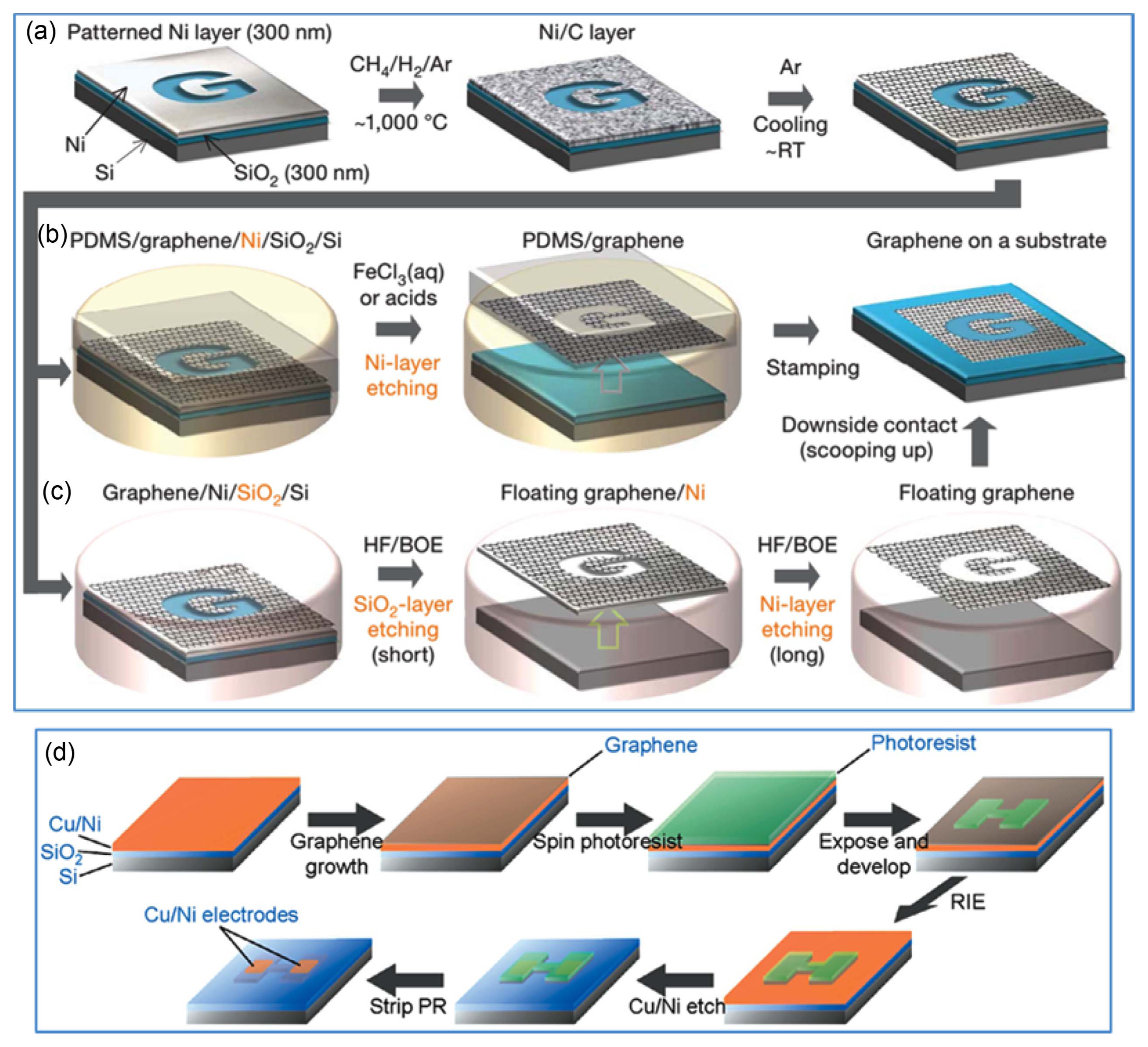
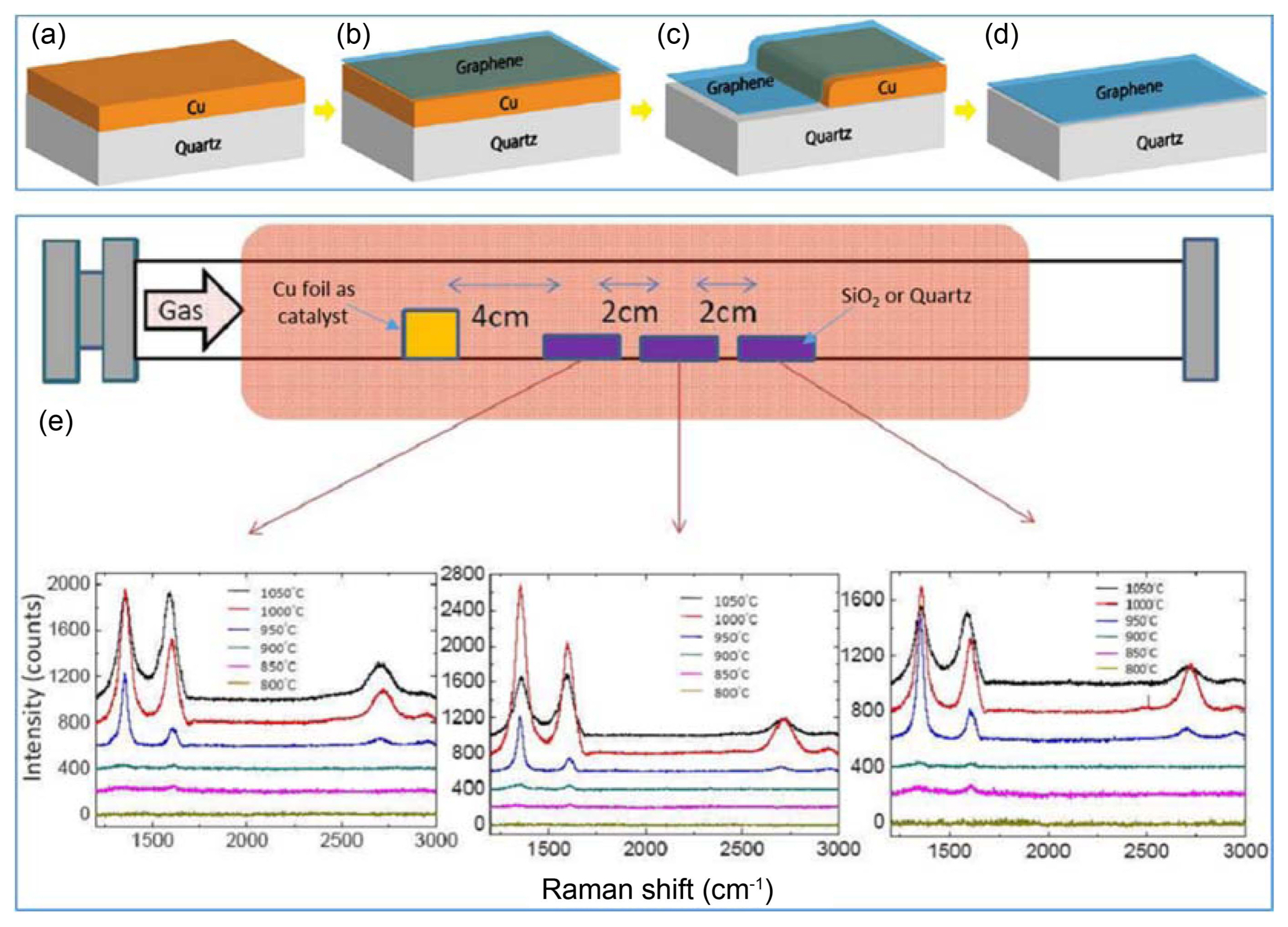
In 2009, the first study on the large-scale direct growth of graphene based on Ni catalysts on SiO2 substrates using CVD was done.39) Thin layer of Ni was deposited on top on SiO to act as catalyst. After graphene growth, it can be transferred by either PDMS stamp/Ni etching or lift off on target substrate by scooping. This method can be used for graphene transfer on flexible and stretchable substrates like polydimethylsiloxane (PDMS) to be used in transparent conducting film (TCF) and field-effect transistor (FET) applications (Fig. 1(a)).39) In this study, of graphene growth on SiO2 was not the best direction; nevertheless, this pioneering study opened up a new direction for direct graphene growth on insulating substrates (h-BN, PDMS, etc.) while avoiding complex transfer processes. The light transmittance, sheet resistance, and electron mobility of the synthesized graphene were 97%, 650 ω/sq, and 3700 cm2V−1s−1, respectively.39) In addition, Levendorf et al. conducted another pioneering study using solid Cu and Ni as catalysts instead of Cu foil under electron-beam evaporation for deposition of graphene on a SiO2 substrate (Fig. 1(b)). After the CVD growth, Cu/Ni etching was performed to obtain a graphene film on the SiO2 substrate with a mobility of 700 cm2V−1s−1.71) In another report, the direct growth of graphene based on Cu deposition by electron-beam evaporation on quartz, sapphire, SiO2, and fused silica substrates was performed (Fig. 2(a)).101) Catalyst evaporation and de-wetting control could lead to the direct patterned growth of graphene and other 2D materials for large-scale electronics. Teng et al. (Fig. 2(b)) presented an interesting direct CVD technique for growth of graphene with high crystallinity on SiO2, comparable to the crystallinity of graphene/Cu foil. The electron mobility (100 - 600 cm2V−1s−1) achieved using this technique was very low.78) However, one problem of this method was the uniformity of the graphene layer, and it may have led to incomplete graphene coverage on the substrate.
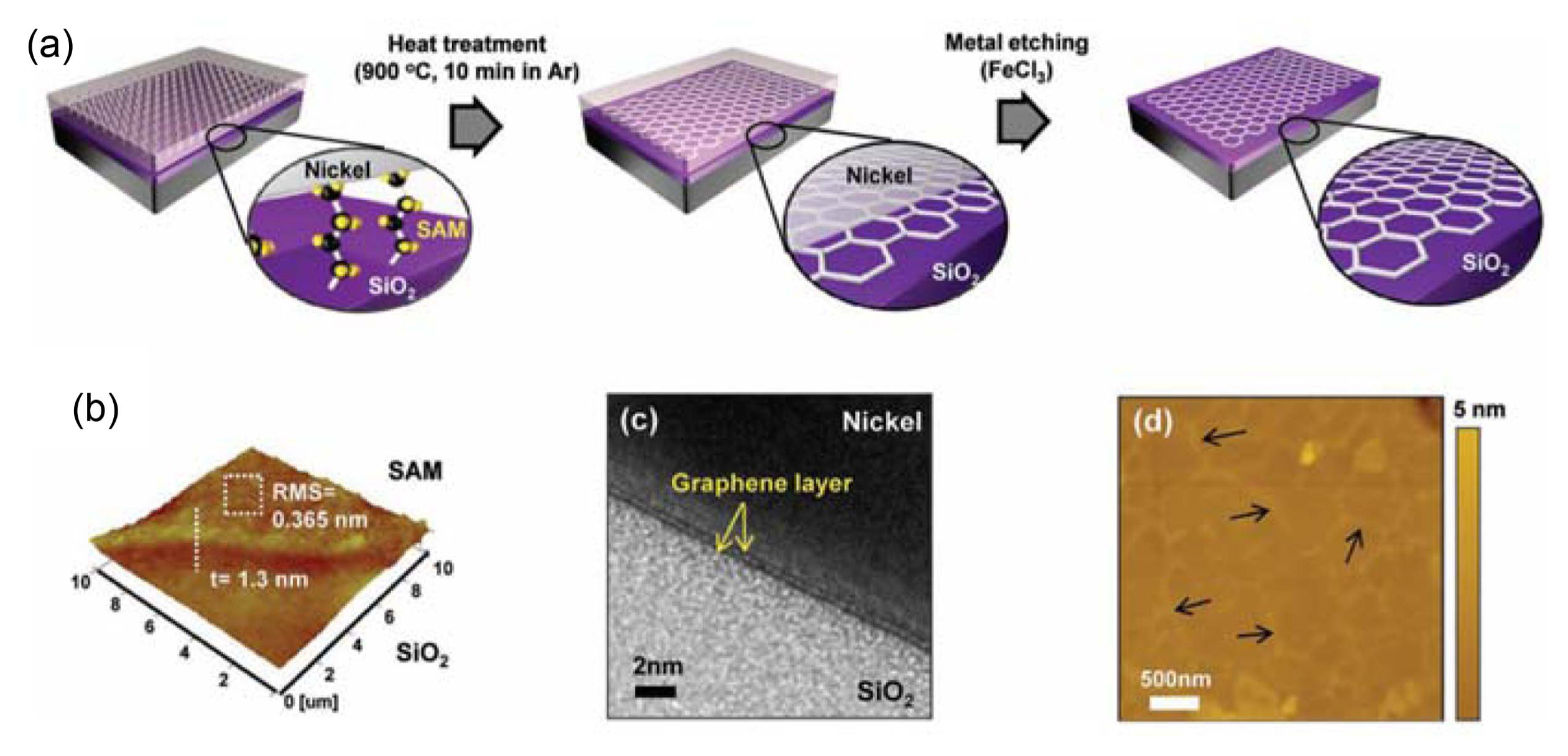
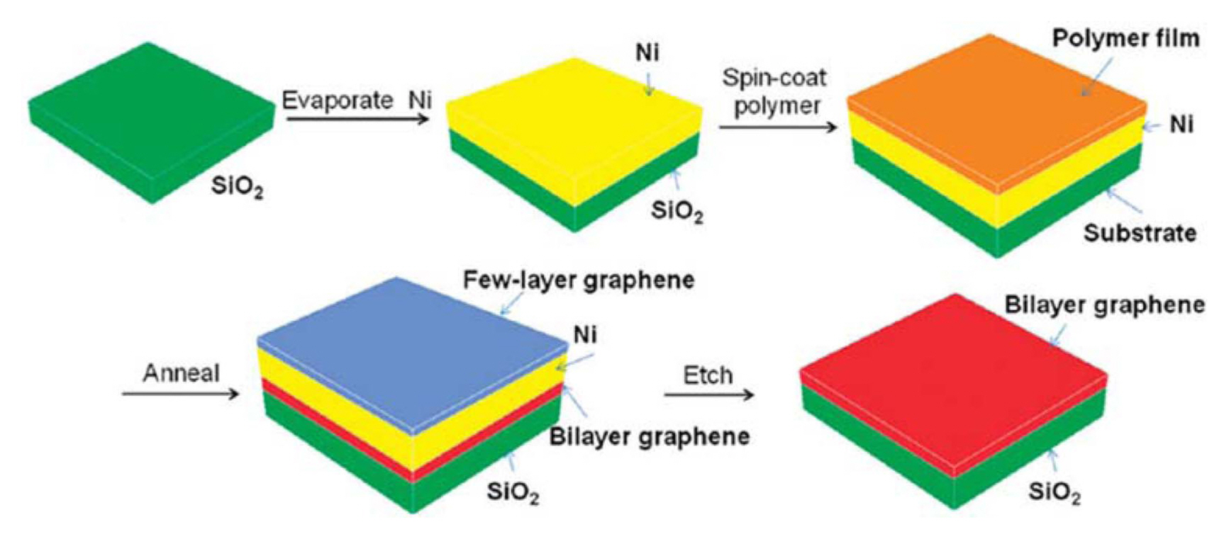
Another effective method that has been studied is the catalytic conversion of an organic layer (a self-assembled layer or a carbon-containing organic thin-film layer) to a graphene layer at the interface between the metal catalyst film and the dielectric ionic substrate to directly grow graphene on dielectric substrates.72,94) This method enables efficient catalytic conversion, allowing the direct growth of low-defectdensity graphene on dielectric substrates. However, the non-uniformity of the grown graphene layer is a drawback. Shin et al. adopted a simple transition-free synthesis of few-layer graphene (FLG) on SiO2 substrates through the thermal decomposition of a carbon-based aliphatic self-assembled monolayer (SAM) polymer using Ni metal as the catalyst, as shown in Fig. 3.70) Because the amount of carbon introduced can be controlled, SAM is considered to be more effective and promising than carbon sources. This Ni/SAM/substrate structure had an advantage in that it could robustly remove the top catalyst during the synthesis process, thus enabling the evaporated SAM chemicals to form high-quality defect-free graphene due to the high-temperature heat treatment. In 2011 Byun et al. demonstrated that catalytic metals such as Ni and Cu can be used for the catalytic conversion of polymer films (polystyrene (PS), polyacrylonitrile (PAN), polymethylmethacrylate (PMMA)) (Fig. 4(a)).72) These polymers are generally available at a low cost and can be used as carbon gas sources during CVD. Using these carbon sources, catalytic pyrolysis (1 min at 1000°C) was performed with a Ni capping film (50 nm thick) used as the catalyst to obtain FLG. More recently, the successful synthesis of FLG exhibiting a light transmittance and sheet resistance of 84.3% and 3.5 kω/sq, respectively, on a desired substrate (SiO2, quartz, GaN, etc.) was achieved using Cu-assisted catalytic conversion of a phenyl-THF polymer (PhSi (OMe)) (Fig. 4(b)).94) This directly grown graphene also exhibited excellent chemical sensitivity to NO2 and NH3.
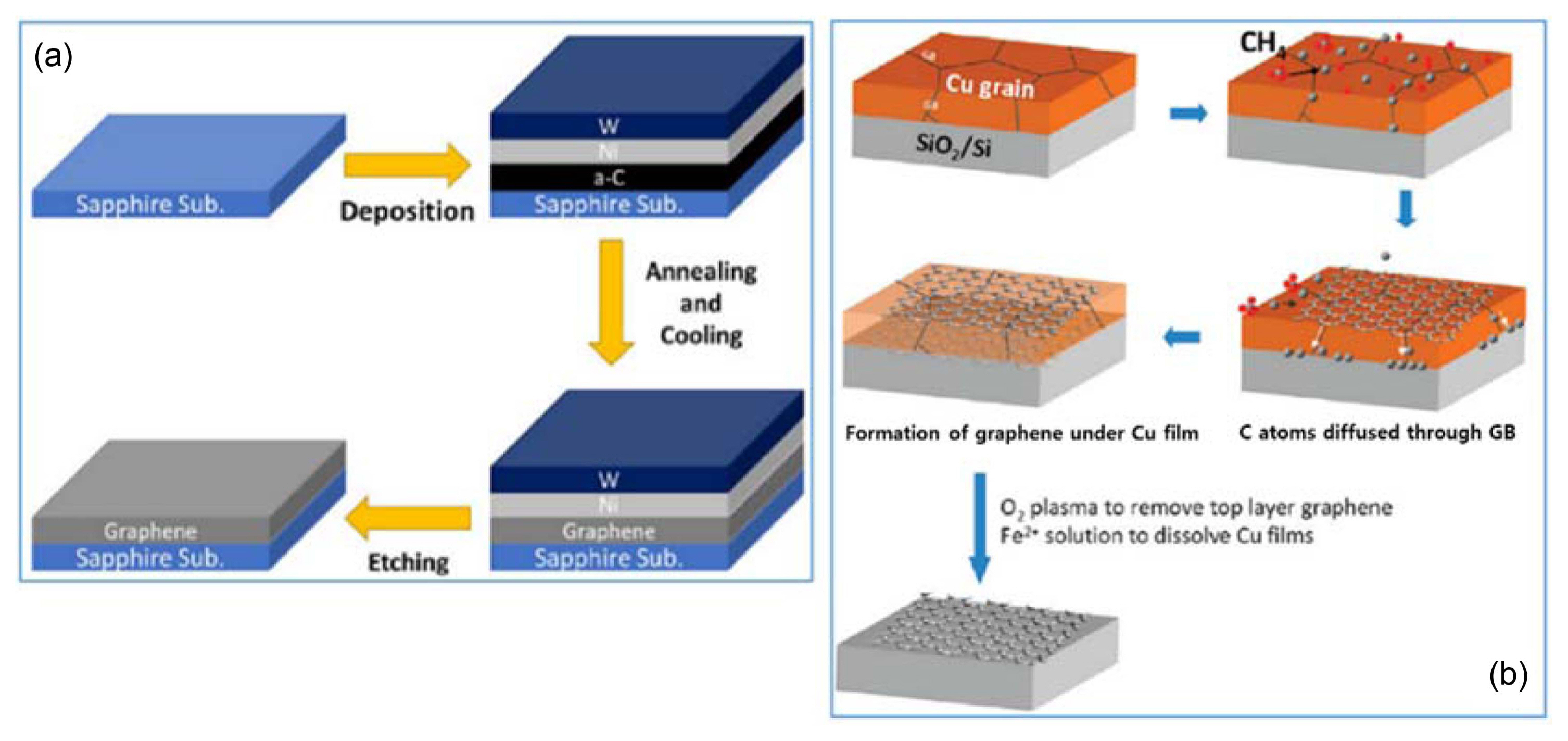
Direct growth of FLG from amorphous carbon sources on sapphire substrates via Ni and tungsten using a thermal evaporation and annealing method was achieved by Yamada et al. (Fig. 5(a)).82) According to this strategy, deposited graphene was sandwiched between W and Ni layers on the top and sapphire on the bottom, as shown in the Raman and differential interference microscopy photographs.82) In another report, graphene was grown directly on quartz and SiO2 via CVD using Cu as the catalyst (Fig. 5(b)).83) This was achieved by the careful optimization of the CVD growth parameters, and the obtained graphene had a mobility of 672 cm2V−1s−1, which is suitable for FET applications.83) In another pioneering study, the direct growth of high-quality bilayer graphene (BLG) on SiO2 assisted by Ni catalyst and carbon sources (PMMA, C8H8, C3H3N, C4H6) was described (Fig. 6).84) At a high temperature (1000°C), the carbon source deposited on the Ni film decomposed and diffused into the Ni layer. When cooled to room temperature, BLG was formed between the catalyst and the substrate. Finally, after the Ni film was etched, BLG was directly obtained on SiO2 without the need for a transfer process. The growth of BLG on SiO2 substrates was investigated by Raman spectroscopy and transmission electron microscopy (TEM) images.84) This approach could lead to BLG-based applications in the near future.
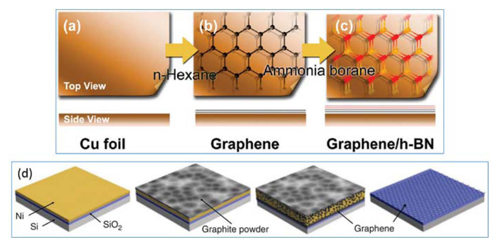
In 2011, Liu et al. selected h-BN as the dielectric substrate for the direct synthesis of highly oriented pyrolytic graphite and mechanically peeled graphene by a two-step CVD method (Fig. 7(a)-(c)).86) h-BN is an ideal dielectric substrate because it is smoother than SiO2 wafer substrates, as shown by atomic force microscopy (AFM) images (scan range: 100 nm) of graphene/h-BN and graphene/SiO2 (with surface roughness values of 0.21 and 0.94 nm, respectively).102) CuH3, hexane solution (C6H14), and ammonia borane (NH3-BH3) were also used as precursors for large-scale synthesis. This approach has opened a new path for exploring the nanotechnology applications of heterostructured graphene/h-BN. Due to the high cost of growing graphene using high-temperature CVD, scientists have attempted to synthesize graphene at very low temperatures both directly and indirectly. However, this aim has faced many difficulties due to the incomplete natural growth of graphene at very low temperatures. Recently, direct growth on SiO2 near room temperature (25 - 160°C) assisted by Ni catalysts has been reported89) (Fig. 7(d)). However, the resulting graphene is of very poor quality.
In principle, it is promising to directly grow graphene on dielectric surfaces using a gaseous catalyst, since low-temperature catalyst growth of low-defect graphene is possible without further etching of the catalyst.
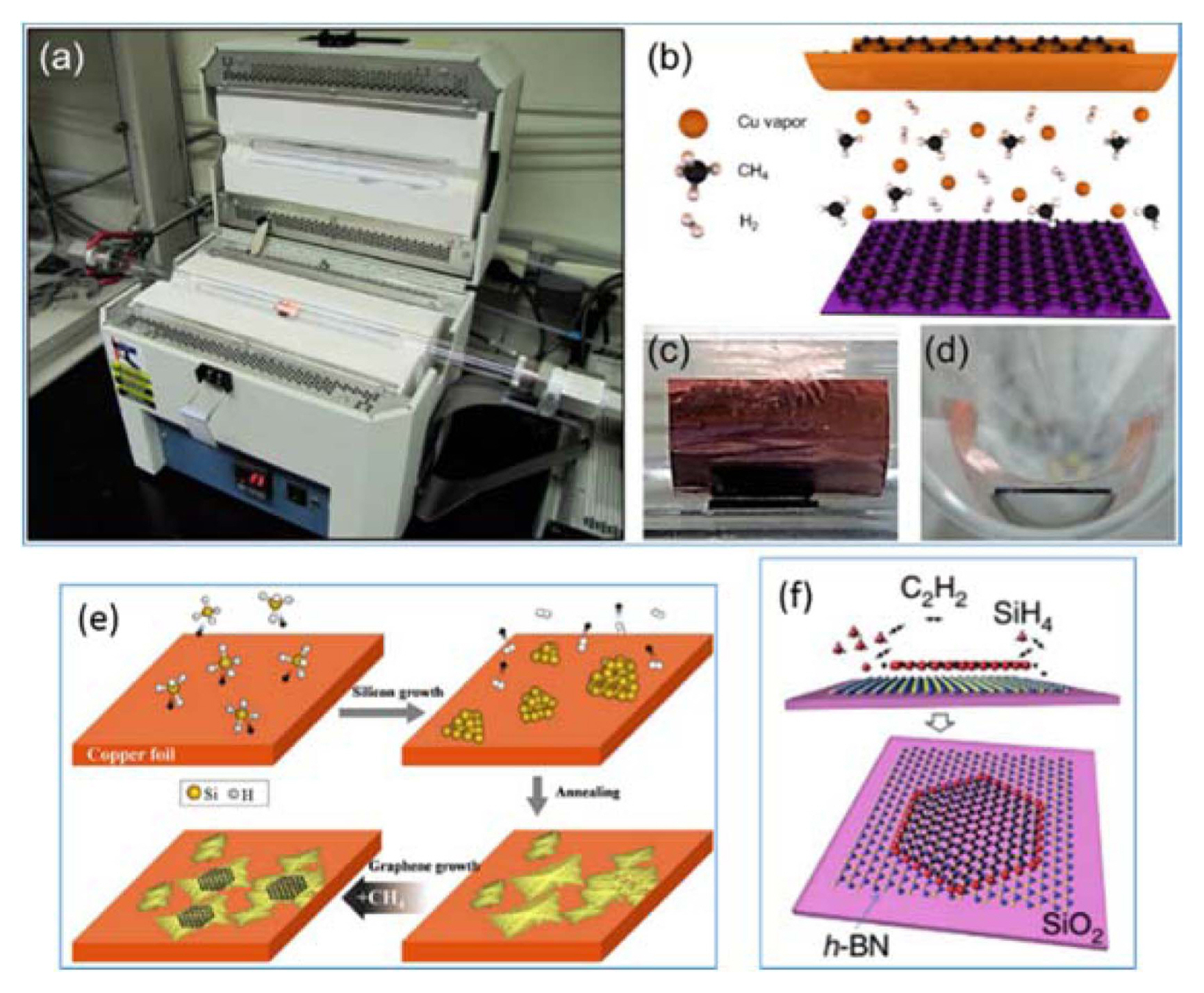
In 2013, Kim et al. reported SLG growth on SiO2 by copper vapor-assisted CVD (Fig. 8(a)-(d)).91) In a more recent report, Li et al. used SiH4 as a catalyst for direct graphene growth by CVD.92) The SiH4 aided the direct deposition of graphene on h-BN and h-BN/SiO2 insulating surfaces and the assembly of Cu foil and SiH4 catalyst inside the CVD chamber (Fig. 8(e)). The best results were obtained by Tang et al. at a growth rate ~ 1 μm/min with a graphene domain size of ~ 20 μm and mobility of ~ 20,000 cm2V−1s−1 (Fig. 8(f )).93)
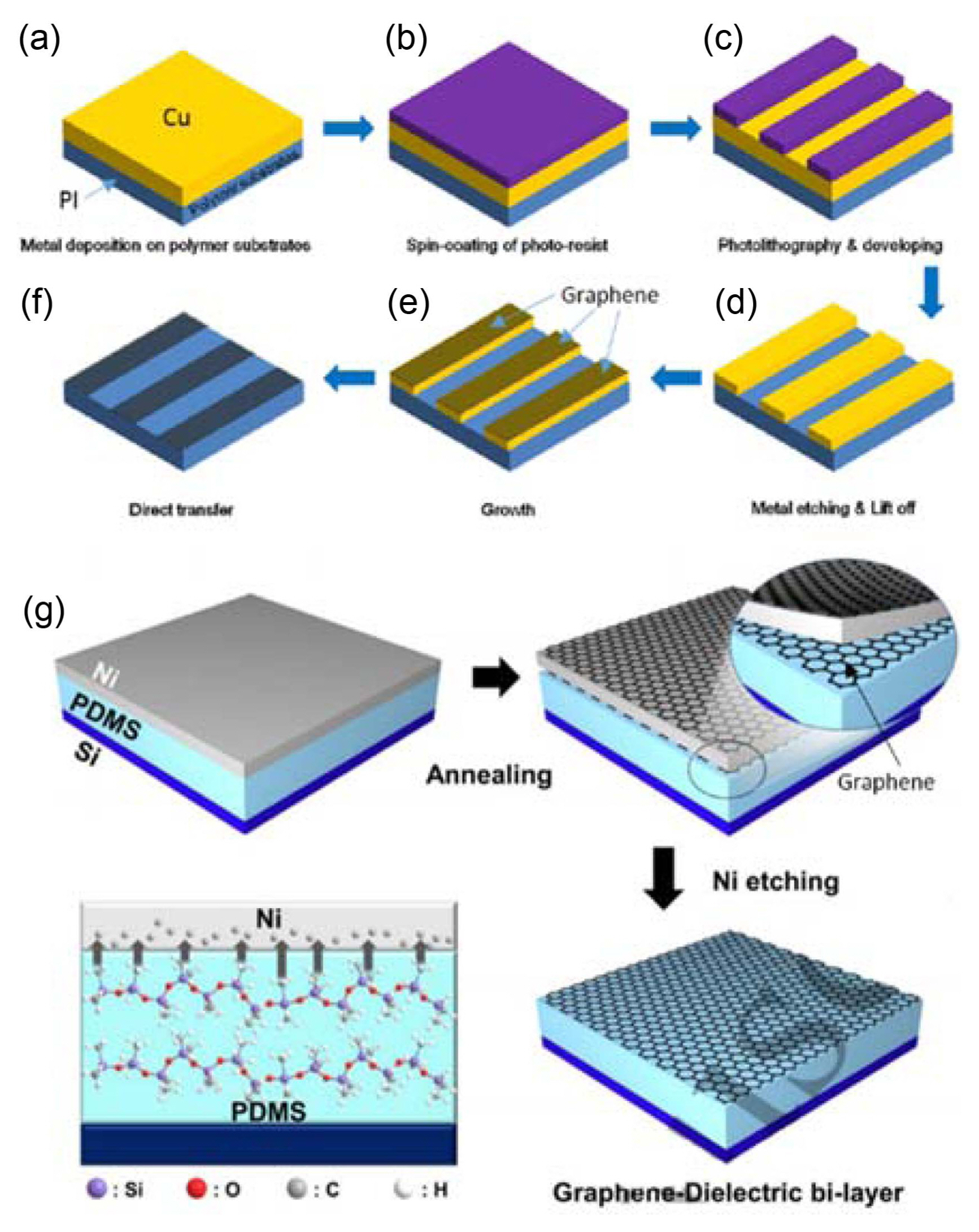
Direct growth of graphene on flexible organic substrates is highly desirable for applications related to flexible and stretchable electronics such as e-skins, biosensors, and health monitors for humans.103,104) However, the limited thermal stability of the organic substrates, which are easily melted, deformed, or damaged at high temperatures (> 300°C), is a serious limitation. So far, the quality of graphene grown at low temperatures (< 400°C) is much poorer than that at high temperatures (~ 1000°C). Due to these constraints, research on graphene growth on flexible substrates has only begun recently.80,81) To reduce the process temperature, most of the studied growth methods involve the catalytic conversion of organic precursors to graphitic layers on flexible organic substrates with the help of catalytic metal layers. In 2012, Kim et al. revealed a low-temperature (300°C) growth method using inductively coupled PECVD and a direct transfer of graphene-graphitic carbon (G-GC) films onto a flexible polyimide (PI) substrate with no additional chemicals (Fig. 9(a)-(f)).80) The optical and electrical characteristics of G-GC were affected by varying growth temperature, plasma power, and growth time. Due to the strong van der Waals forces and π-π interactions at the interfaces between the G-GC films and the PI substrate, the patterned G-GC films were not facially detached or damaged on the substrate after wet etching and transferring. More recently, in 2016, Seo et al. revealed a simple, scalable, inexpensive, and patternable process to synthesize graphene-dielectric bilayer (GDB) films from solution-processed PDMS under a Ni capping layer (Fig. 9(g)).81) Here, Ni films were deposited as the catalyst and the encapsulation layer on the PDMS layer had a thickness of a few micrometers. This layer enabled the direct growth of GDB between the substrate and the Ni layer. PDMS (4 μm)/Ni (400 nm) films on the substrate were thermally annealed using a vacuum furnace to form a PDMS/multilayer graphene (MLG)/Ni/MLG structure. At the interface of the PDMS layer and the Ni film, the carbon atoms on the PDMS surface diffused into the Ni layer at high temperatures, and the carbon atoms were released to form MLG on both sides of the Ni layer during cooling. This method was used to fabricate GDB simultaneously and directly on the substrate by the thermal conversion of PDMS without using additional graphene transfer and patterning processes or without forming an expensive dielectric layer, thus making the device fabrication process much easier.
3.2. Non-catalytic growth
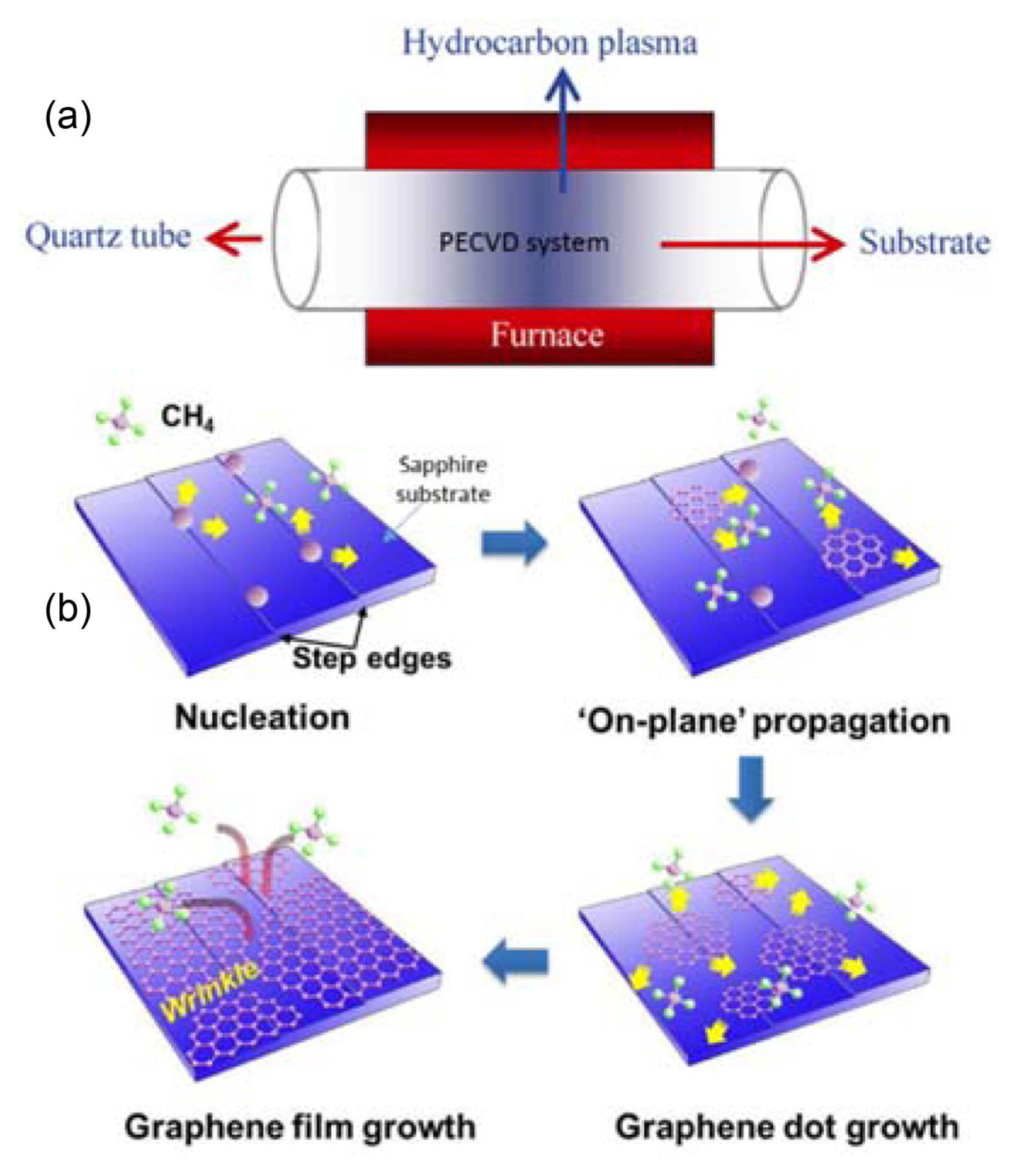
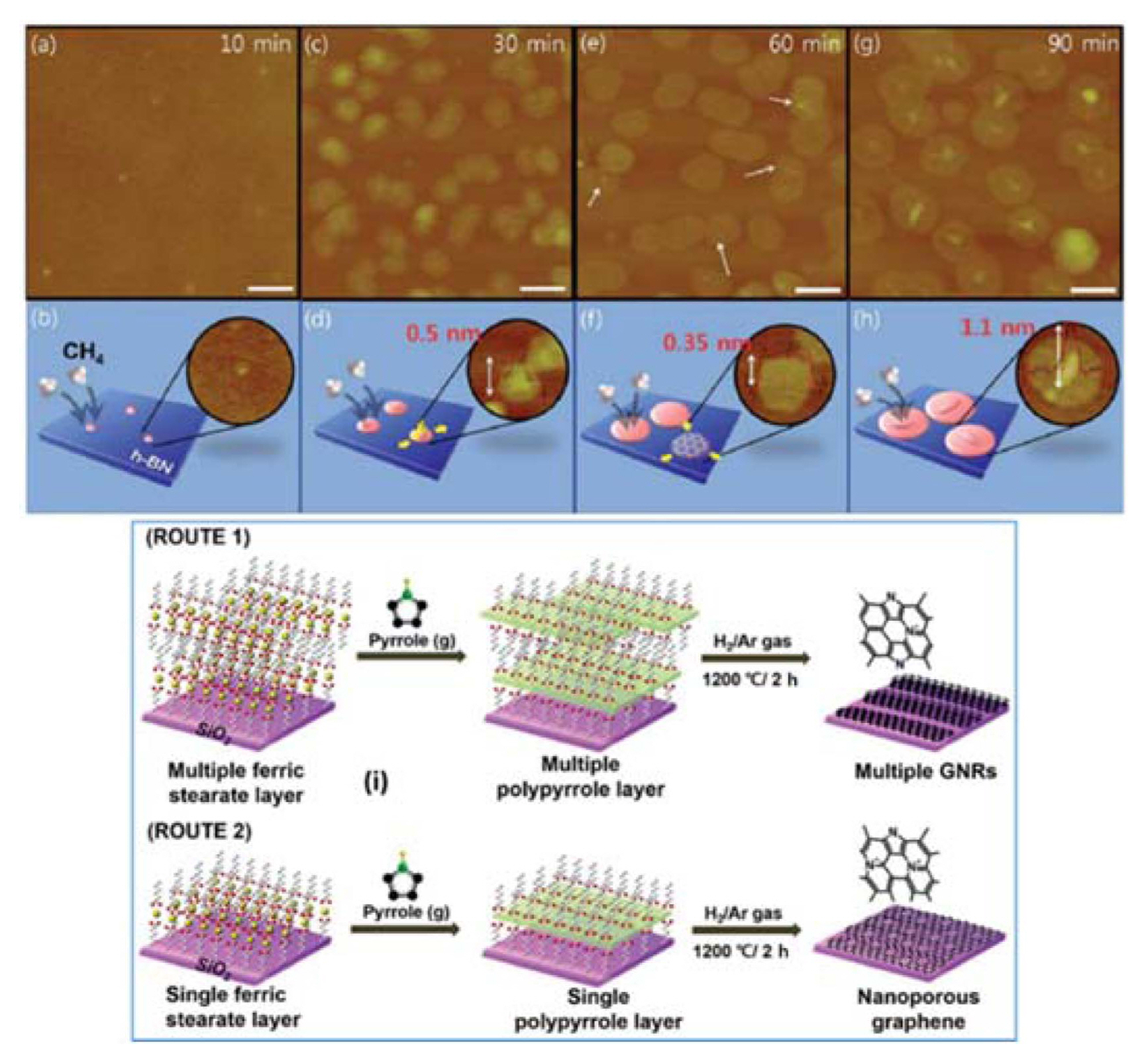
Direct growth of graphene on arbitrary substrates without the need of an additional catalyst is advantageous due to the fewer processing steps required and lower processing cost. However, this approach is limited by low activation energy; as a result of this low energy, chemical reactions related to graphene growth cannot successfully obtain uniform high-quality graphene for commercialization compared to existing synthesis processes. In 2011, Zhang et al. reported the use of a remote PECVD system at low temperature (500°C) for the direct growth of graphene on various inorganic dielectric substrates (sapphire, quartz, mica, Si, SiC, glass) (Fig. 10(a)).68) This method was cost-effective, simple, scalable (up to 4-inch wafers), and compatible with devices such as nanoresistors, gas sensors, and TCFs. In another report, Song et al. demonstrated catalyst-free direct growth of large-scale SLG on sapphire without graphene transfer using high-temperature (950°C) CVD (Fig. 10(b)).76) In 2011, Son et al. reported catalyst-free direct growth of graphene in a horse-pad shape with a diameter of up to ~ 110 nm on a mechanically exfoliated h-BN surface placed on a SiO2 substrate through ambient-pressure CVD (APCVD) (Fig. 11(a)-(h)).105) Moreover, this study indicated that graphene growth involved nucleate particle formation, and BLG was formed as an instantaneous state during SLG growth on h-BN via a peripheral process.105) Most recently, Min et al. reported a new technique for catalyst-free bottom-up growth of graphene nanoribbon (GNRs) and nanoporous sheets based on the pyrolysis of SAMs of ferric stearate molecules directly onto SiO2 substrates.85) The GNRs containing pyrrolic N-enriched edges obtained by this method exhibited p-type semiconductor properties, whereas the nanoporous graphene sheets containing inhomogeneous pores and graphitic N-enriched basal planes exhibited n-type semiconductor properties (Fig. 11(i)).85) It was expected that this direct graphene growth technique could be applied to various graphene-based electronic applications without the requirement for graphene transfer. However, the drawback of this method was the high-density defects of the GNRs, which were confirmed by the high D peak in their Raman spectra.85)
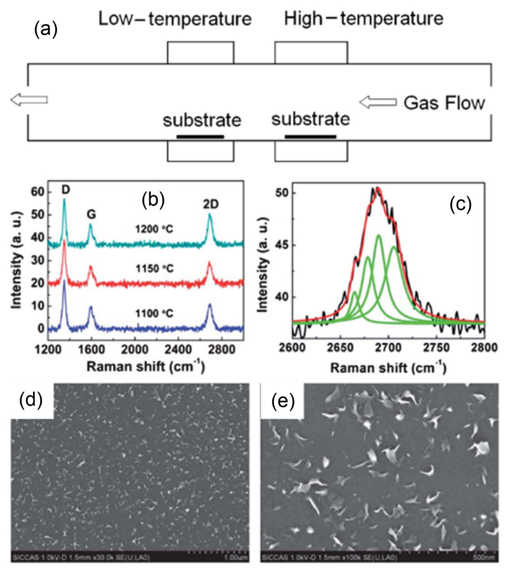
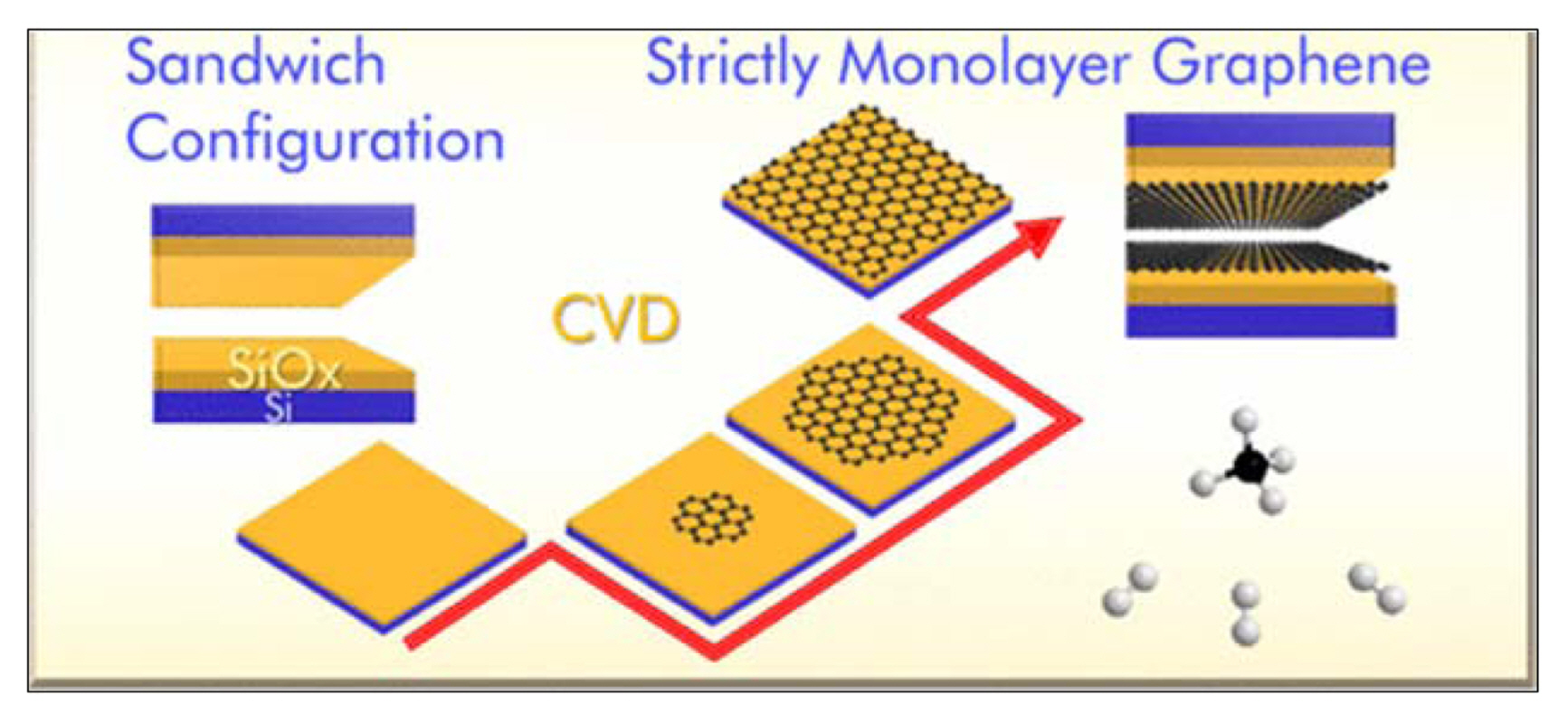
In 2016, Song et al. reported the direct growth of conformal graphene films on 3D quartz surfaces, which could be applied to pressure sensors.55) This 3D graphene layer grown on the quartz surface had excellent electrical and optical properties, with a sheet resistance of ~ 2000 ω/sq and light transmittance of ~ 80% at 550 nm, which could be attributed to the presence of a flat graphene film on the PDMS substrate; the obtained film could be used as a pressure-sensitive sensor. Trung et al.,87) Xu et al.,88) and Bi et al.90) showed the direct growth of graphene on Si, SiO2, quartz, AlN, and h-BN substrates without a catalyst support. Xu et al. used CVD with two temperature zones for the direct growth of uniform and continuous graphene layers, as shown in Fig. 12(a).88) High-temperature CH4 dissociation provided the active carbon species required for low-temperature graphene growth. As a result, the graphene grown directly on the transparent quartz substrate showed a reasonably good light transmittance and sheet resistance of 97% and 650 ω/sq, respectively.88) These values reported by Xu et al. were almost similar to those reported by Bi et al. (94% and 425 ω/sq, respectively, using PECVD) (Fig. 12(b)-(e)).90) These CVD and PECVD techniques could synthesize transfer-free graphene for future high-performance electronic devices. In another report, using remote electron cyclotron resonance plasma-assisted CVD (650°C), Munoz et al. directly grew graphene on insulating substrates (quartz, SiO2) at low temperature.97) Through the sophisticated control of the growth parameters (e.g., nucleation density, edge growth, thickness), Munoz et al. obtained highly crystalline graphene monolayers exhibiting a light transmittance of ~ 92% and sheet resistance of ~ 900 ω/sq.97) In early 2017, Pang et al. reported a new method based on direct self-terminating confinement on two sandwiched Si/SiOx substrates for large-scale growth of uniform graphene monolayers (Fig. 13).98) This result is a significant advancement for transfer-free graphene growth, considering that the transfer-free synthesis of “extremely uniform” graphene as a monolayer or bilayer is a significant challenge.
In 2015, Sun et al. reported the catalyst-free direct growth of uniform graphene on various solid glass substrates (quartz, borosilicate, sapphire) using cost-effective APCVD and its potential for daily-life applications such as heat-resistant devices, photocatalytic plates, and energy-saving smart windows, as shown in Fig. 14.99) This is one of the pioneering studies for the direct well-controlled large-scale growth of high-quality graphene on insulating solid glass. Sun et al. discovered that the light transmittance and sheet resistance values of the synthesized graphene could be facially compatible together with the experimentally tunable layer thickness of graphene.99) In 2010, Rummeli et al. investigated a new facile strategy for the direct growth of graphene on a MgO dielectric substrate using hexane (C6H14) as the catalyst via very-low-temperature (325°C) CVD.67) These graphene films were well formed and confirmed MgO to be a suitable dielectric substrate for direct graphene synthesis via CVD at 325°C without the requirement for a transfer process. This approach has considerable potential for large-scale fabrication of future Si-assisted devices.
4. Low-temperature Growth
So far, most graphene growth processes have used methane as the precursor to produce high-quality graphene monolayers at temperatures of ~ 1000°C. To overcome the difficulties encountered during high-temperature growth processes using methane, the use of other solid or liquid hydrocarbon precursors has recently received considerable attention. As a result, the growth temperature of graphene has greatly decreased to as low as 300°C by adopting alternative carbon sources such as hexane, ethanol, ethylene, pentane, alcohol, and benzene for thermal CVD and PECVD. The obtained graphene structures have been analyzed using advanced techniques and have been adopted for the fabrication of multifunctional devices.
4.1. Adoption of liquid precursors
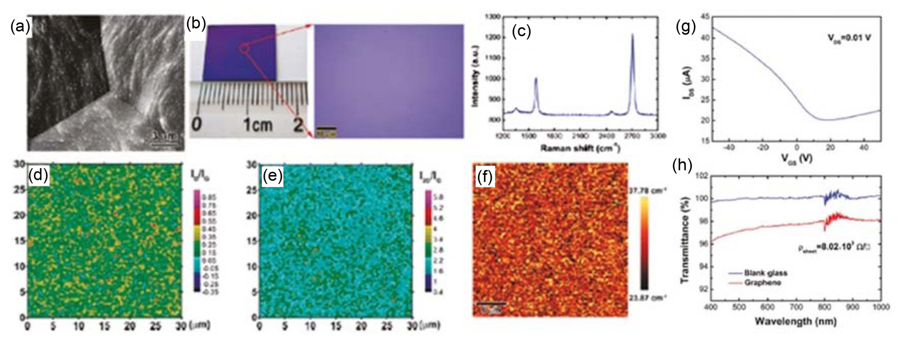
Graphene monolayers were obtained using thermal CVD at a growth temperature of around 1050°C and ultra-low pressure.61,106) Further, graphene monolayers with a similar quality were synthesized by Zhang et al. using toluene as the precursor via low-pressure CVD at a low growth temperature of 600°C.107) In this study, copper foil, which was used as the substrate, was electrochemically polished before deposition and ultrahigh-purity hydrogen and toluene were used at flow rates of 3.3 sccm and 2.7 mLh−1 respectively. The partial pressure was maintained at 300 mTorr during the reaction. The Cu thin film was annealed at 980°C for 15 min and then grown in two steps. It was grown at the desired temperature (300 - 600°C) for 60 min initially and then the growth was continued at a 10-fold higher pressure maintained by closing the throttle valve for 5 min. A continuous graphene film grown on Cu electropolished at 600°C in two stages is shown in Fig. 15; as is clearly visible in the optical image, the graphene film is transferred to a Si/SiO2 substrate. According to Raman analysis, the 2D/G peak ratio was about 2.18 and the 2D full maximum at half width (FWHM) value was about 36 cm−1. It indicated that the as-grown graphene was composed of a fault with considerably low defects. Confocal Raman spectroscopy mapping over a 30 × 30 μm2 region confirmed that the as-grown structure was a single layer. FETs with a channel width of 300 mm exhibited depletion-type characteristics with p-type conductivity. The electron and hole mobilities of these graphene samples were measured to be 190 and 811 cm2V−1s−1, respectively. This structure exhibited a light transmittance of 97.33% at a wavelength of 550 nm and a sheet resistance of 8.02 × 10³ ω/sq.
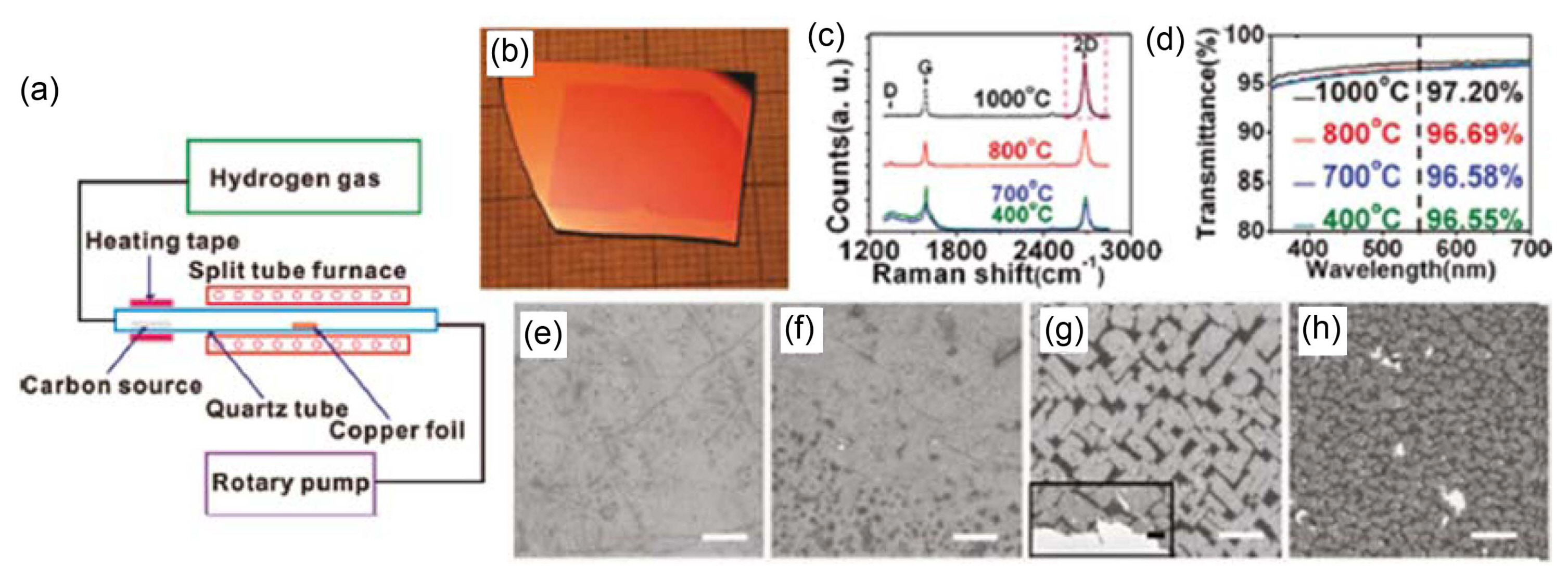
Jang et al.108) demonstrated the growth of a continuous SLG structure on a copper foil substrate via oxide-free CVD using benzene as the precursor. One of the biggest obstacles to the growth of high-quality graphene without the use of amorphous or oxidized carbon layers is the presence of residual oxidizing species in the CVD growth chamber. To overcome this problem, growth was performed in an oxygen-free APCVD system. In a typical process, high-quality continuous graphene sheets were synthesized on a copper foil at 300°C. Here, the aromatic benzene molecules entering the reaction chamber were adsorbed on the surface of the copper foil, causing a catalytic dehydrogenation reaction that formed highly reactive six-ring species and graphene nuclei, as depicted in Fig. 16. Electron microscopy and optical microscopy images of the as-grown graphene showed that the growth of the graphene layer on the copper foil was continuous and uniform. Raman spectral analysis of this structure showed the presence of SLG with few defects. Studies on graphene growth time showed that graphene quality and surface coverage increased with increasing growth time. The graphene structure grown for 5 min exhibited 100% surface coverage and a uniform I2D/IG value of ~ 2, but BLG and MLG flakes were formed in the monolayer over longer durations. FETs fabricated on Si/SiO2 substrates with Ti/Au contacts exhibited typical transistor characteristics. This measurement showed that the graphene structure grown at 300°C exhibited low sheet resistance (1 kω/cm) and high electron and hole mobilities (1900 and 2500 cm2V−1s−1, respectively).
4.2. Adoption of solid precursors
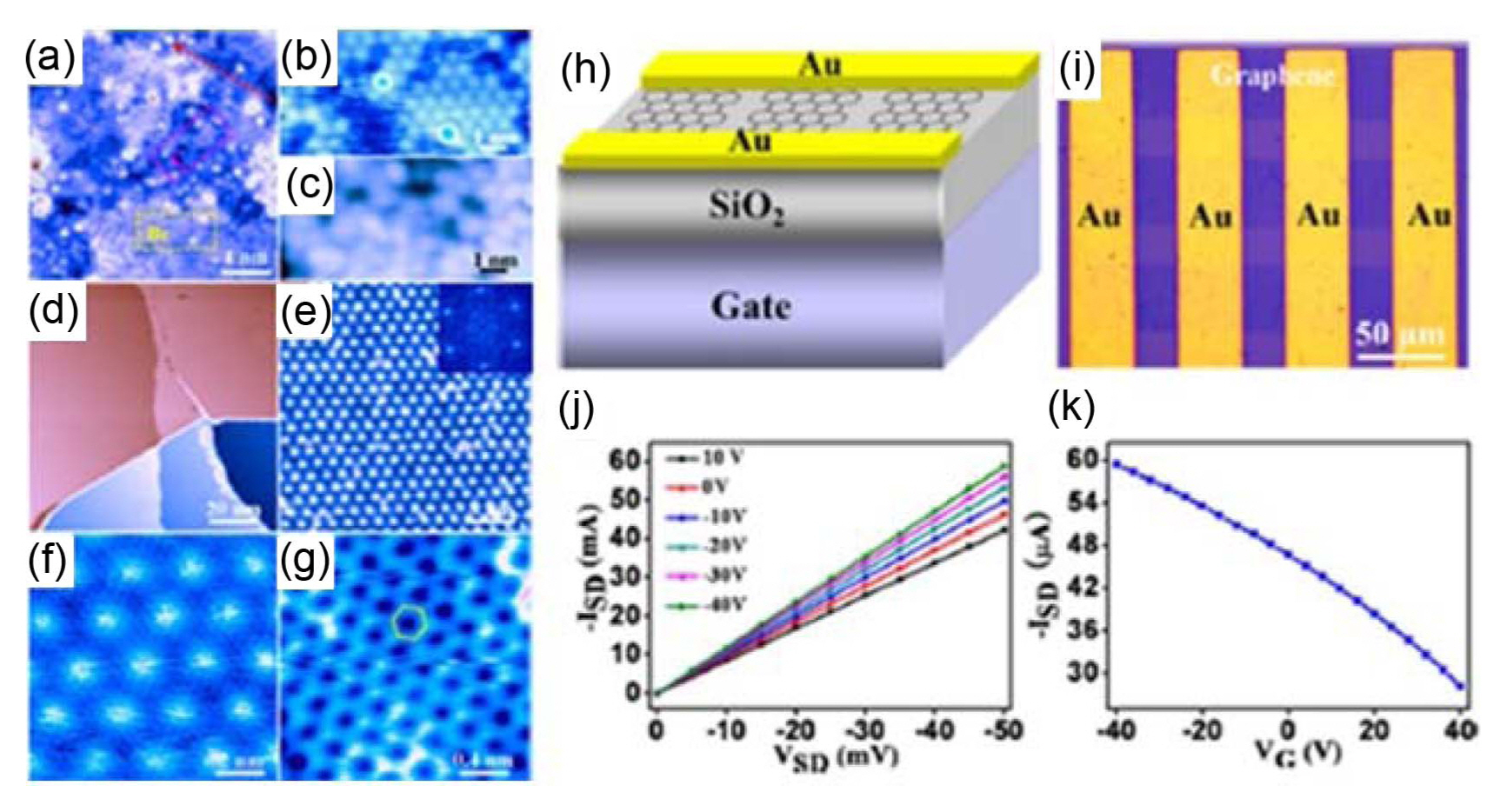
A graphene monolayer structure was developed on a copper foil using a solid carbon source at a pressure of 8 - 15 Torr and a flow rate of 50 sccm for 45 min.66) When the precursor was changed to liquid benzene, the growth temperature significantly decreased to 300°C, while high-quality graphene structures were produced at 800°C using solid PMMA (or PS). As shown in Fig. 17, a typical feedstock gas was supplied by placing a solid precursor (PMMA or PS) individually on the gas inlet side of the growth tube. High-quality SLG was synthesized at 1000 and 800°C using PMMA as the raw material. When the growth temperature was lower than 800°C, a disordered hydrocarbon structure was observed together with graphene.
A mild radical-induced growth of graphene structures was achieved by Jiang et al.109) at lower growth temperatures (220 - 250°C) using a two-zone furnace. The growth of graphene over Cu(111) surfaces was performed by evaporating hexabromobenzene (HBB) under ultra-high vacuum conditions using a Knudsen cell. Here, HBB molecules, which were deposited at room temperature, underwent debromination through Ullmann reaction catalyzed by the copper surface, and bromine adatoms aggregated in hexagonal closely packed islands (Fig. 18). As a result, the decomposed carbon atoms aggregated into disordered clusters. However, high-quality graphene structures were realized on the Cu(111) surface by depositing HBB at 570°C. Electrical characteristics of the as-grown graphene structures evaluated using FETs fabricated on Si/SiO2 substrates exhibited mobilities in the range of 1000 - 4200 cm2V−1s−1. The overall results clearly indicated the high quality of the graphene structures.
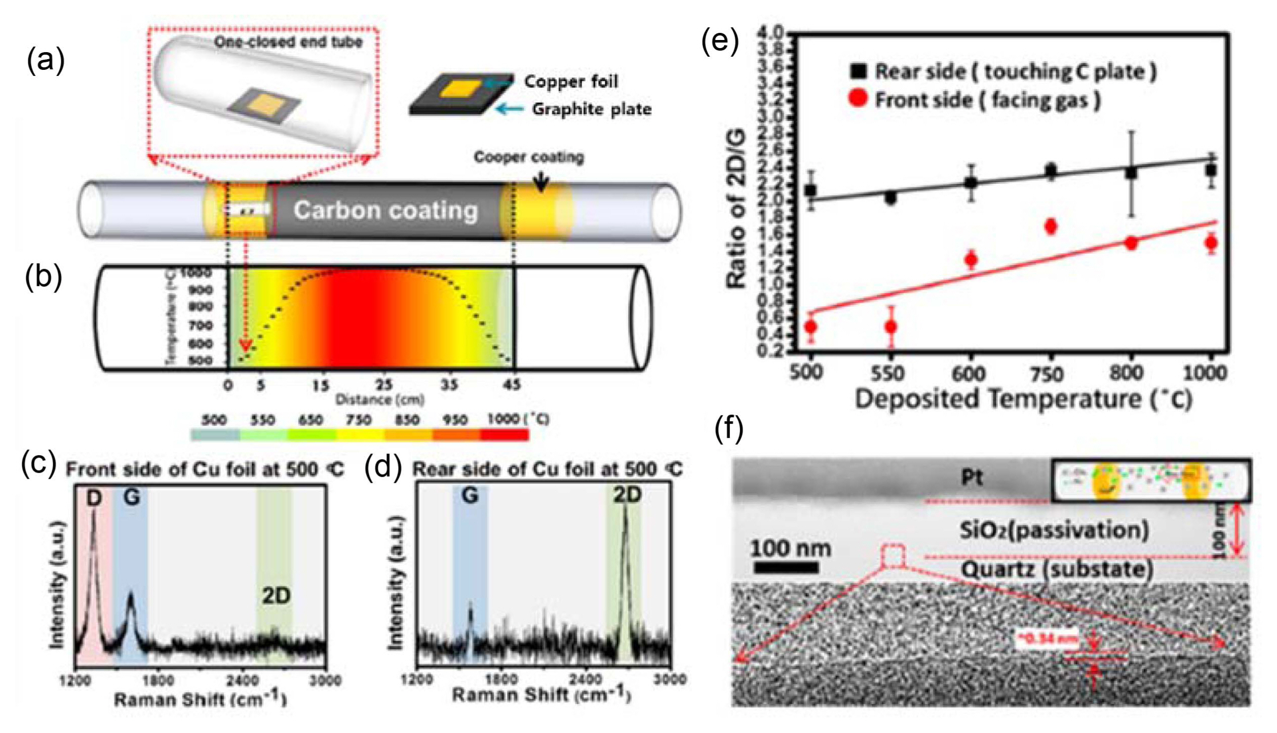
High-quality SLG structures were obtained using carbon-containing CVD (CE-CVD) processes at very low temperatures of 500°C.110) Low-temperature CE-CVD was used for SLG growth (Fig. 19). The graphene structure grown on the entire surface of the Cu foil showed a very strong D peak, but the graphene structure on the backside of the foil had a FWHM of ~ 35 cm−1, indicating a very strong 2D peak and I2D/IG ratio of approximately 2. This result highlighted that the graphene structure grown on the backside of the Cu foil was composed of high-quality SLG. While lowering the growth temperature from 1000°C to 500°C, the reduction in the I2D/IG ratio was negligible, indicating that the SLG quality at 500°C was similar to that achieved at 1000°C. This result emphasized the importance of graphite holders for copper catalyst behavior, which greatly improved the growth of SLG.
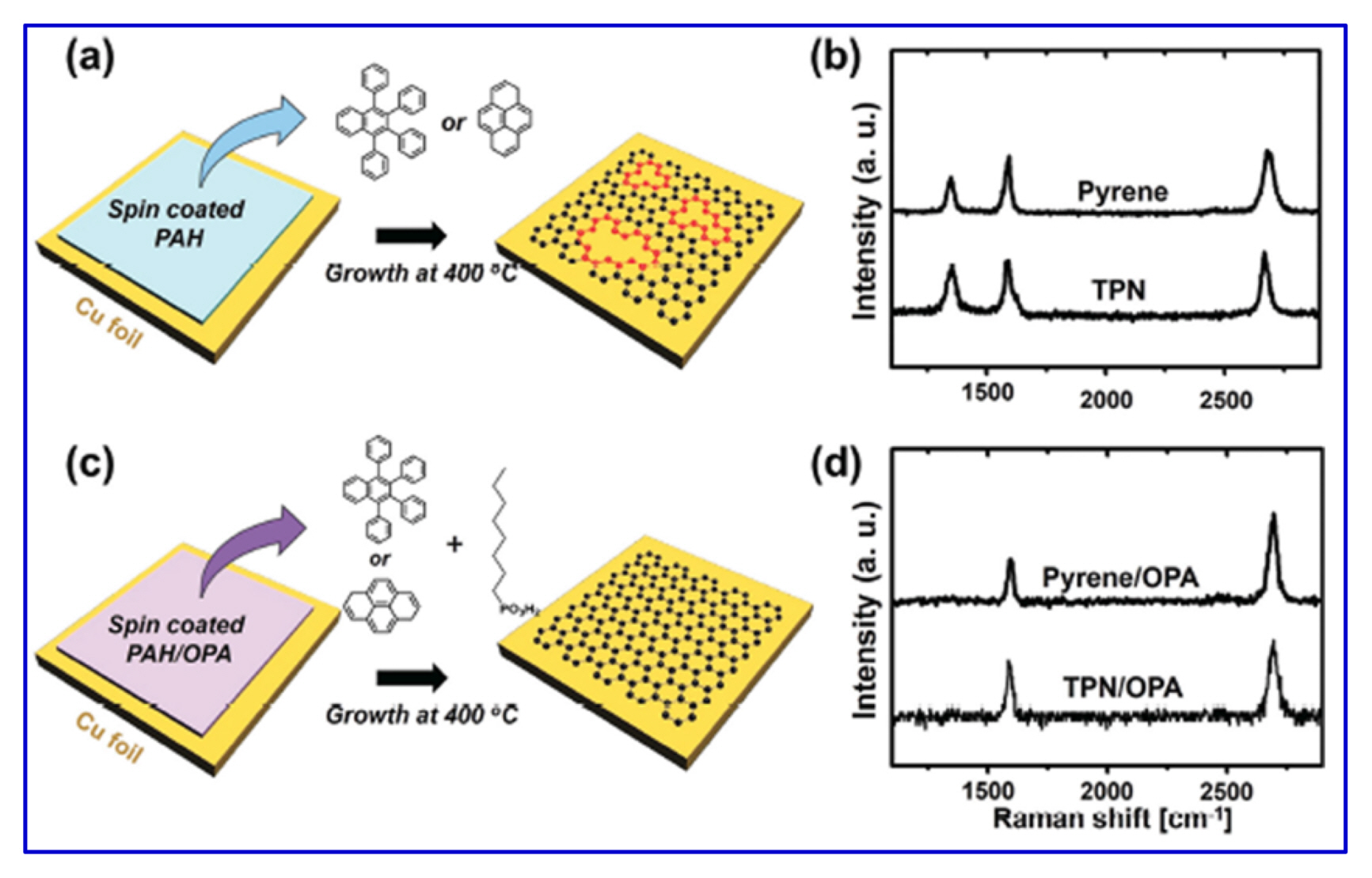
The temperatures required for graphene growth are significantly lowered by the use of polycyclic aromatic hydrocarbons (PAHs) because the activation energy between the metal substrate and PAHs is reduced, which is important for the dehydrogenation of precursors and subsequent nucleation.111,112) However, graphene growth at low temperatures using PAHs results in numerous quality-related defects, making it difficult to be integrated into electronic devices and other applications.113) To address this issue, Lee et al.114) proposed a novel approach that allows low-temperature graphene growth and reduces number of defects. They used a mixture of PAHs with aliphatic carbon sources instead of PAHs alone as the precursors to grow graphene at low temperatures. The aliphatic carbon neutralized the defects related to the native graphene structure by introducing small carbon fragments on the surface of the substrate. As the result, the graphene structures formed defect-free monolayers.
PAHs and 1-octylphosphonic acid (OPA) were added to the substrate and graphene growth was conducted in a CVD system at 400°C under a pressure of 0.15 Torr for 90 min. The Raman spectrum of the graphene structure grown using the PAH source (Fig. 20) showed peaks at 1580 cm−1 and 2700 cm−1 with D and D′ peaks at 1350 and 1617 cm−1, respectively. The ID/ID′ ratio was 4, indicating that the as-grown graphene structure was composed of vacancy-type defects. On the other hand, the Raman spectra of the other samples showed negligible D peaks, indicating that the graphene grown using the PAH + OPA source consisted of a high-quality monolayer. TEM analysis showed that graphene grown using PAH alone consisted of a hexagonal array of carbon atoms formed as a monolayer. Notable defects were observed at 1012 cm−1. However, as shown in Fig. 21, the structure grown with OPA alone showed amorphous carbon fragments. These were mainly caused by the conversion reaction of PAH-derived carbon fragments rather than OPA-derived carbon fragments. On the other hand, the structure grown under an optimized OPA-doped PAH source represented a six-membered carbon hexagonal ring, and the grown structure was high-quality SLG. The FET study of both structures also showed that the structure grown with the PAH + OPA source exhibited significantly higher hole and electron mobilities of 1000 and 800 cm2V−1s−1, respectively. Thus, these results demonstrated that the quality of the as-grown graphene structure using the PAH + OPA source was sufficient for use in electronic devices.
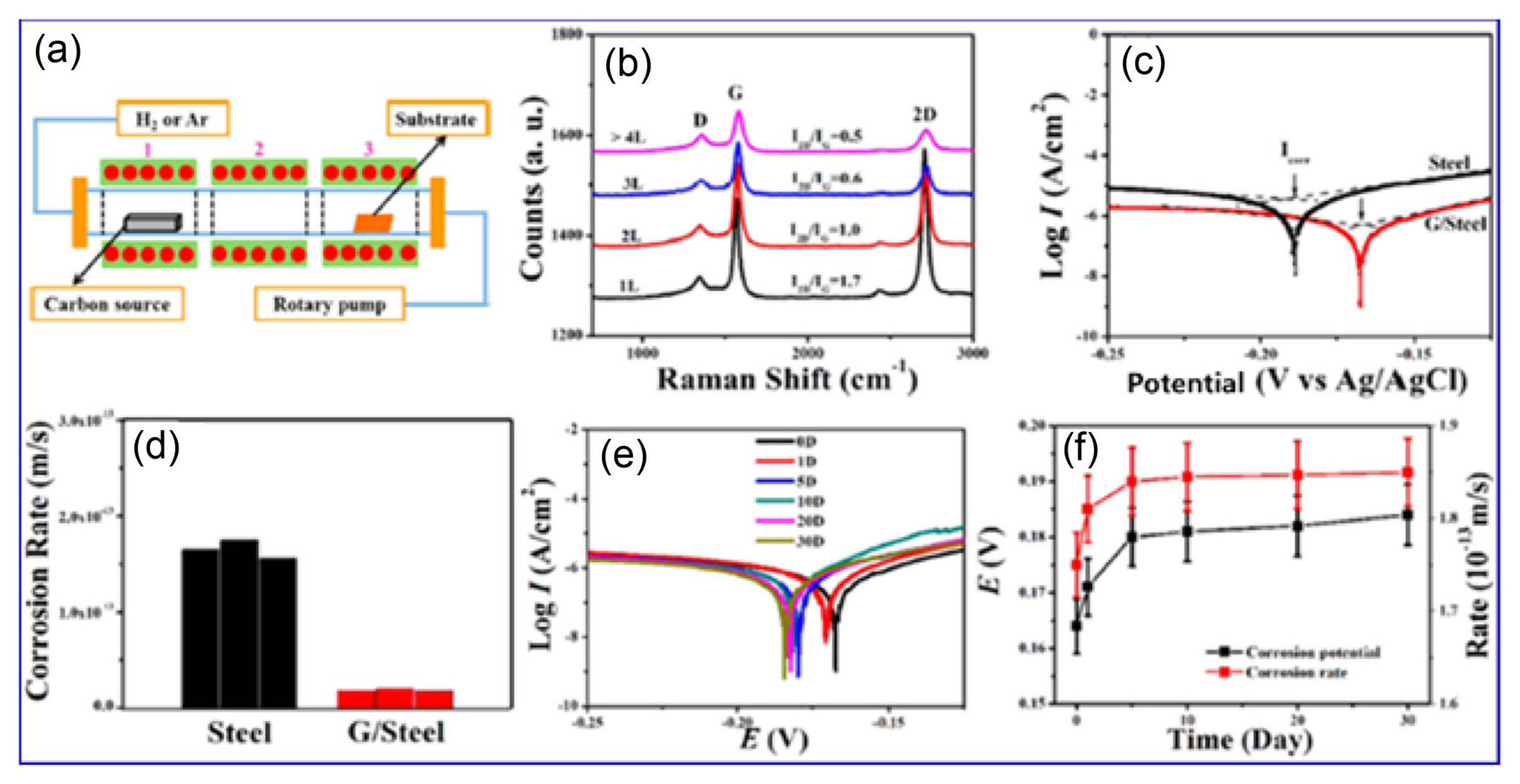
Graphene is considered to have excellent anti-oxidation and -corrosion properties because of its chemically inert nature, resulting in graphene-coated objects being protected from corrosion even in an extremely harsh environment. Zhu’s group115) used multi-heating-zone CVD to synthesize graphene on stainless steel substrates from a solid carbon source (Fig. 22). Prior to graphene growth, the stainless steel substrate was annealed at 700°C for 5 min under a constant H2 flow of 200 sccm. The graphene growth was performed after annealing at a temperature of 500°C under H2 and Ar atmospheres at a total pressure of 2 mTorr. The Raman spectra of these graphene structures showed the presence of BLG to FLG. However, graphene structures grown at high H2 flow rates, i.e., > 40 sccm, consisted of SLG only. The stainless steel sheets covered by the graphene structures under optimal growth conditions were used as the electrode for the quantitative analysis of corrosion rates using Tafel analysis. The cyclic voltammetry (CV) curves of stainless steel coated with graphene shifted to lower potentials and the current decreased significantly compared to that of bare steel. The corrosion rates for the graphene-coated and bare stainless steel sheets were 2.02 × 10⁻¹⁴ and 1.75 × 10⁻¹³ ms−1, respectively. These results emphasized the significant anti-corrosion ability of graphene-coated steel electrodes despite being grown at much lower temperatures. The corrosion rate slowly became stable with time on immersing the electrodes in a sea salt solution for 30 days. Quantitative and qualitative studies showed that stainless steel coated with graphene layers had up to 10 times lower corrosion rates than their bare counterparts.
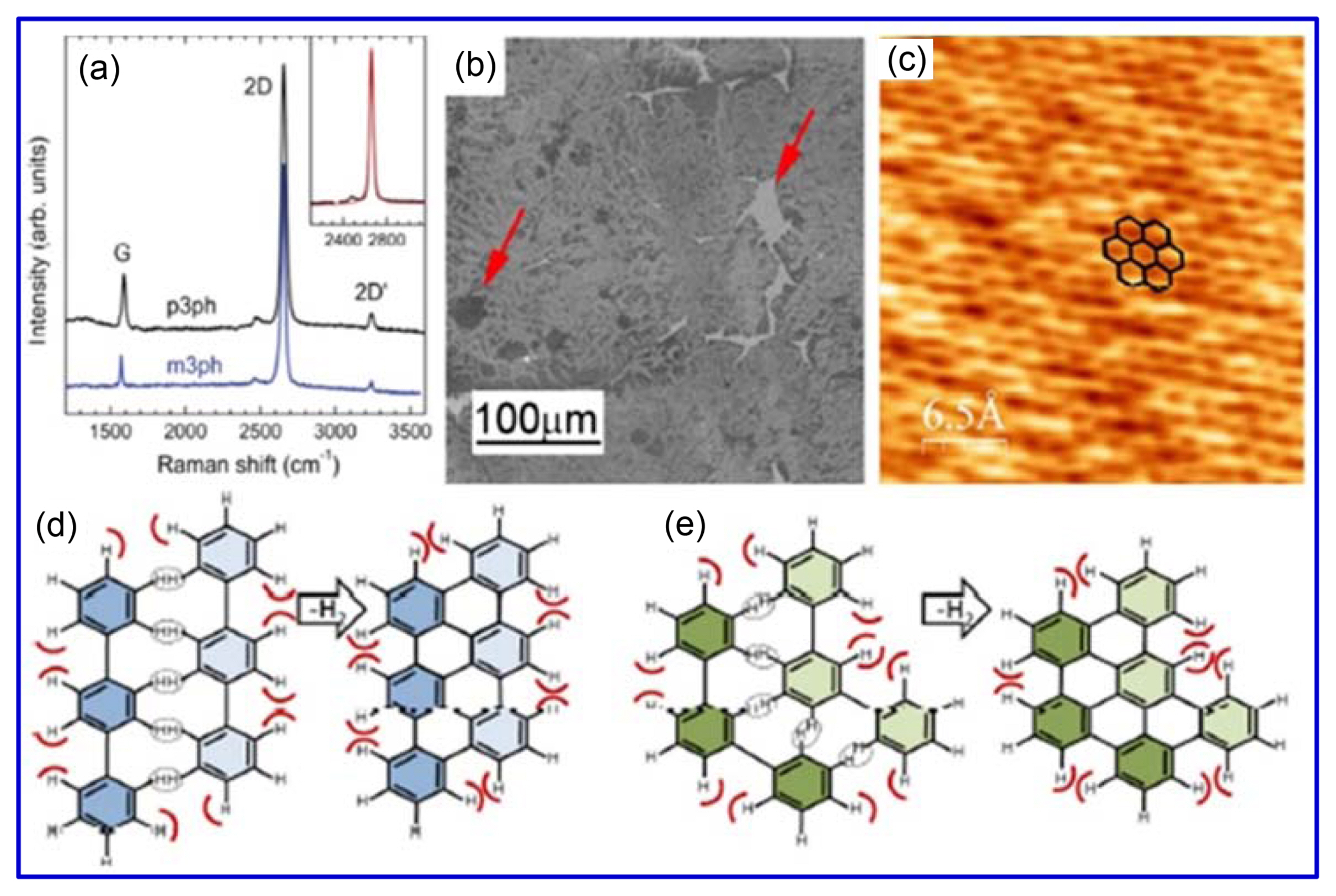
The importance of the structure of the precursor and the intermediate reactions during graphene growth on metal substrates was demonstrated116) by the examination of solid aromatic precursor molecules (anthracene and terphenyl). All experiments were conducted in a CVD system using copper foil as the substrate at 400°C for 20 min under a constant pressure of 4.5 × 10⁻⁶ Torr. The Raman spectra of graphene grown by m- and p-terphenyl (m3ph and p2ph, respectively) are shown in Fig. 23. A narrow 2D peak with a FWHM value of 26 cm−1 and an I2D/IG ratio of ~ 2.5 was observed, which clearly indicated that the graphene structures grown using m3ph and p-terphenyl precursors were single-layered. Surface topography studies revealed that the growth over a copper surface led to almost complete graphene coverage. A highly regular hexagonal structure was observed by scanning tunneling microscopy (STM) analysis. The growth mechanism of graphene could be broken down to the below steps based on the abovementioned results. Initially, the m3ph or p-terphenyl precursor molecules were adsorbed on the surface of the copper foil with a specific adsorption energy because of London dispersion forces,111) which greatly influenced the geometry of the adsorbent molecules. These dispersion forces favored molecules with a tilted configuration when under equilibrium of repulsive forces between C-H bonds. The active sites from the C-H bonds polymerized with adjacent molecules to enable further C-C fusions. These newly formed extended aromatic systems with stronger dispersion forces, i.e., polymerization, decreased the total energy of the system and the inter-molecular coalescence continued, ultimately leading to the formation of a graphene structure. The hydrogen atoms linked with the aromatic C-H structure in this system remained as active sites for the subsequent attachment of other molecules.117) These results demonstrate and emphasize that precursor geometry and molecular structures are key requirements for graphene growth.
4.3. Adoption of gaseous precursors
Graphene growth on single-crystal nickel(111) substrates using ethylene as the precursor via CVD at a partial pressure of 10−6 Torr was realized.118) Based on in situ microscopy studies, it was evident that the structures grown at temperatures below 650°C exhibited thermal stability, whereas those above this temperature exhibited deformation. This temperature was identified as the upper limit for graphene growth over nickel surfaces. Therefore, the self-limiting monolayer growth of graphene on nickel surfaces could be realized by maintaining the growth temperature below 650°C. Apart from uniformity and monolayer growth over a large-area nickel surface, the presence of nickel carbide along with graphene was especially obvious at temperatures below 460°C. This was probably attributed to the self-reconstruction(s) of the nickel surface upon adsorption of carbon according to the in-plane conversion mechanism.119) As a result, a significant rotation (~ 3°) between graphene and the underlying nickel surface was observed.120) To explore these issues, Patera et al.121) studied graphene growth over nickel(111) surfaces by in situ STM and X-ray photoelectron spectroscopy. The growth was conducted at temperatures of 400 - 600°C by exposing ethylene (C2H4) at a pressure of 7.5 × 10⁻⁵ Torr in an ultrahigh vacuum system. The results showed that two key atomistic mechanisms occurred on the Ni(111) surface when it was exposed to hydrocarbons at around 500°C. Below 500°C, conversion of two different nickel carbides led to graphene growth, whereas above 500°C, graphene predominantly grew directly on the Ni(111) surface through replacement mechanisms, leading to embedded epitaxial growth along with rotated graphene domains, as shown in Fig. 24.
Growth of high-quality curved graphene structures on nickel templates at a growth temperature of 650°C using thermal CVD was realized.122) In a typical process, a nickel-containing crucible was heated in a hot-wall tube furnace to 650°C under Ar and H2 flow rates of 300 and 30 sccm, respectively, for 20 min. Then, 5 sccm of methane gas was introduced for 10 min, and the system was cooled down to room temperature. A schematic demonstration of the growth of curved graphene structures using CVD is shown in Fig. 25. At a desired temperature, methane decomposed over the nickel particles as carbon atoms and dissolved into nickel particles. Upon cooling, the carbon atoms precipitated over the nickel particles and formed curved graphene. Fig. 25 also shows the TEM images of the curved graphene structures grown over a nickel template at 650°C. These results revealed that the as-grown graphene consisted of few-layered or multilayered structures. Electrochemical studies of the curved graphene structures, measured in 3 molL−1 KOH aqueous solution, showed a quasi-rectangular CV profile without any redox peaks. It indicated that the graphene structures consisted of very few surface functional groups. The quasi-triangular charge-discharge curves indicated electrical double-layer electrode characteristics. The specific capacitance of the curved graphene structure was found to be 203 Fg−1 at a current density of 1.63 Ag−1. Linear increase in the discharge current through the electrodes with an increase in the scan rate indicated efficient charge transport and ion diffusion in the electrodes, which were attributed to the high conductivity and excellent electrochemical properties of the curved graphene structures.
5. Summary and Future Challenges
A brief review of the first direct growth of graphene on any dielectric flexible and rigid substrate through CVD with or without metal and polymer catalysts is presented in the first part of this study. By making direct graphene growth possible on the target substrate, research on the optimal growth conditions and growth mechanisms in current CVD systems is being conducted. In addition, direct growth of graphene has made it possible to apply graphene in the fields of CMOS technology, energy devices, pressure sensors, transparent conductors, bio-devices and wearable devices. It is necessary to study the correlation between graphene layer number and graphene quality, which is considered to be an existing challenge for direct graphene growth. In fact, the number of graphene layers can be finely controlled and should be selected with reference to the thickness variation and growth time of the metal catalyst. This is essentially a much better demonstration of direct graphene growth on dielectric substrates. The prospect for direct graphene growth has received considerable consideration from the 2D material research community as the “most important issue” when developing new transfer-free graphene for direct manufacturing. Various heterostructured devices are applicable using this direct growth technique.
The challenge of direct growth of graphene is low quality. In addition, for industrial applications, the current technology of CVD systems is not large-scale and limited to small area, but current systems for direct growth of graphene are difficult to apply industrially as the quality of directly grown graphene is inferior to that of graphene obtained by conventional indirect growth. An enormous breakthrough in ultra-modern technology and an accurate understanding of the growth mechanisms of graphene synthesis systems are essential. To achieve this, studies on the growth mechanism and layer number control of graphene have been actively conducted.81,84) The results obtained today have not yet met expectations and require more effort from the 2D material community. This aim represents an extreme desire as a “secret issue” to achieve the ultimate goal of a large, defect-free graphene-based ultra-low-power electronic device that can be commercialized over the next 20 years.
The second part of the article explores recent low-temperature graphene growth techniques. Significant efforts have been made to grow a continuous layer of high-quality graphene over a large area. For low pressure CVD (LPCVD), high-quality graphene can be obtained by altering the carbon precursor (solid, liquid, and gas sources depending on the decomposition temperature) or metal catalysts (Cu, Ni, CuNi) for low-temperature growth (~ 500°C). In the case of PECVD, the reduced temperature for growing SLG is about 450°C, which is obtained by changing the plasma type and plasma power used. Due to the formation of faults during low-temperature graphene growth, the overall results of device grade quality and desired size are very poor. Also, there has been little research on the direct growth of a graphene layer on a desired substrate. Moreover, application-based investigation on graphene monolayers conducted so far has been scarce. This is due to the lack of a methodology for growing SLG of the required quality and size directly on a non-catalytic substrate at low temperatures. However, intensive efforts are underway to demonstrate innovative solutions to existing obstacles, and the future generation can undoubtedly benefit from this amazing material.
The low-temperature growth of graphene greatly reduces the production cost and facilitates the development of various devices. However, the main shortcomings of low-temperature growth are the quality, uniformity, crystallinity, and size of the obtained product. It is very difficult to maintain good properties when the graphene structure grows at low temperatures. It is also important to obtain a single layer with growth homogeneity over a large area. Designing a new methodology to overcome this problem of the development of graphene faults is very difficult. In addition, a detailed understanding of the dynamics of low-temperature growth is required, as well as interface and device integration with other materials.
Graphene is a promising material, but its adoption in device manufacturing is still in its nascent stage. An important issue to solve is that it cannot be grown directly on high-resistance and non-catalytic materials. With advances in low-temperature graphene growth and direct growth on the desired substrate/material, efficient adoption of low temperature or directly grown graphene for device integration is still not very efficient and additional developments are required to utilize full potential of graphene on arbitrary substrates. In addition, the transfer of graphene onto a desired substrate requires a transfer process, which leads to defect formation and other problems. For nanoelectronic devices, the graphene transfer process is more complicated and prone to defects. Although there have been some reports on the direct growth of graphene, the growth temperature is still high, which is another major obstacle for graphene integration in nanoelectronics. Therefore, the direct growth of graphene at low temperatures is highly desirable. Thus, multidisciplinary techniques should be researched with a focus on developing methodologies to grow device-quality graphene structures at significantly lower temperatures. To date, graphene growth and low-temperature growth have been actively studied. However, to further increase the applicability to future graphene devices, it is necessary to identify a technique for directly growing graphene at lower temperatures. Graphene low-temperature/direct growth technology is expected to realize the application of graphene in various industries and to expand the commercial application fields of graphene.