


1. Introduction
In the recent past, one-dimensional (1D) nanostructures with nanometer diameters, such as nanowires, nanorods, and nanotubes, have attracted increased interest due to their optical, electrical, and mechanical properties. Potential applications range from probe microscopy tips to interconnections in nanodevices. Therefore, current researchers have focused on developing industrial methods and improving available applications for large-scale synthesis of high-quality crystalline nanostructures.1-3) Silicon carbide (SiC) is an important wide band gap semiconductor with superior properties, such as high breakdown field strength, high thermal conductivity, high saturation drift velocity, and excellent physical and chemical stability.4) The use of modern SiC technologies has led to a rapid improvement in the material quality of SiC and has made practical SiC devices a reality. Researchers from different fields have proposed several approaches, such as carbon-nanotube confined reaction, chemical vapor deposition, laser ablation, arc discharge, sol-gel methods, and carbothermal reduction for growth of 1D SiC nanostructures using bottom-up processes.5-9) There exist multiple methods for growing 1D SiC whiskers and wires, but controlling stacking faults and other defects during synthesis still remains a challenge. Stacking faults are usually found in 3C-SiC structures and affect their various properties.10) Seo et al. preformed studies on various morphologies and stacking fault insertions in SiC whiskers grown using carbothermal reduction.11) They successfully controlled the morphologies and fault angle in SiC whiskers for use as a reinforcement in composite materials. In this study, we synthesized β-SiC nanowires with diameters in nanoscale range on a porous body and silicon wafer substrate using low-grade silica and carbon black powder via carbothermal reduction at 1400°C. We then investigated their structural characteristics.
2. Experimental Procedure
In carrying out the carbothermal reduction process for growth of SiC nanowires, we used a vacuum furnace (10−2 - 10−3 Torr, 2400°C maximum temperature) with inert Ar gas. Lower grade silica (purity: 97.5%, Samchun Pure Chemical Co., Korea) and amorphous carbon black powder (Purified Carbon Black, < 200 nm, SUPELCO, USA) were chosen as the starting materials as they have the advantage of inducing high reactivity. The starting materials were fabricated using the porous bar-type (5 × 1 × 0.5 cm3) green body mixed with silica and carbon black powder with 1 : 3 wt% ratio. The porous green body enabled material sources to be evaporated for growth of SiC nanowires in the carbothermal reduction process. An Si substrate (wafer with (100) exposed plane) was located close to the porous body in order to compare the nanowires grown on the porous body (PBSiC) and those grown on the Si wafer (SWSiC). SiC nanowires were grown at 1300 - 1600°C temperature, 30 - 180 min holding time, and Ar gas flow rate in the 500 - 2,000 sccm range. However, we chose SiC nanowire samples that were grown at temperatures below 1450°C because the Si substrate melted at higher temperatures. Ar gas was introduced to maintain an inert atmosphere during the heat-up period. After the furnace was cooled to room temperature, a gray layer on the porous body surface and light green layer on the Si wafer surface were observed.
The morphologies of PBSiC and SWSiC nanowires were observed and analyzed using scanning electron microscopy (SEM; Tescan Vega TS 5136XM, Czech Republic). X-ray diffraction (XRD; Rigaku-GDX-XRD, Rigaku Co., Japan) was used to determine the crystalline phases and measure and compare the stacking fault content in the nanowires.10) Stacking faults in individual nanowires were characterized using high-resolution transmission electron microscopy (HRTEM; Tecnai G2 F30 S-Twin, FEI, USA)) images and selective area electron diffraction (SAED) patterns. Energy dispersive spectra (EDS) were obtained using an HRTEM equipped with an energy-dispersive spectroscopy (EDS) system.
3. Results and Discussion
In order to grow 1D SiC nanowires by carbothermal reduction, we started with a porous body composed of silica and carbon black powder. The overall reaction in the porous body between each of the powders for producing SiC is as follows:
In fact, Eq. (1) proceeds through two stages in which silicon monoxide (SiO) gas is formed as a vapor phase intermediate. The first step consists of a solid-solid or solid-liquid type of reaction between carbon and silica, leading to the formation of silicon monoxide and carbon monoxide (CO) vapor phases according to Eq. (2). Eq. (3) shows the second step, where silicon monoxide subsequently reacts with carbon to form SiC. Silicon monoxide obtained from Eq. (2) reacts with carbon to yield SiC nuclei heterogeneously on the surface of carbon, which is the commonly accepted mechanism of bulk SiC formation.12) However, the vapor-liquid-solid (VLS) growth mechanism is well-known. Silicon-carrying and carbon-carrying liquid droplets are formed by melting metallic catalysts that were added intentionally. The evaporated silicon and carbon atoms diffuse across the droplet and deposit to form SiC nanowires.13)
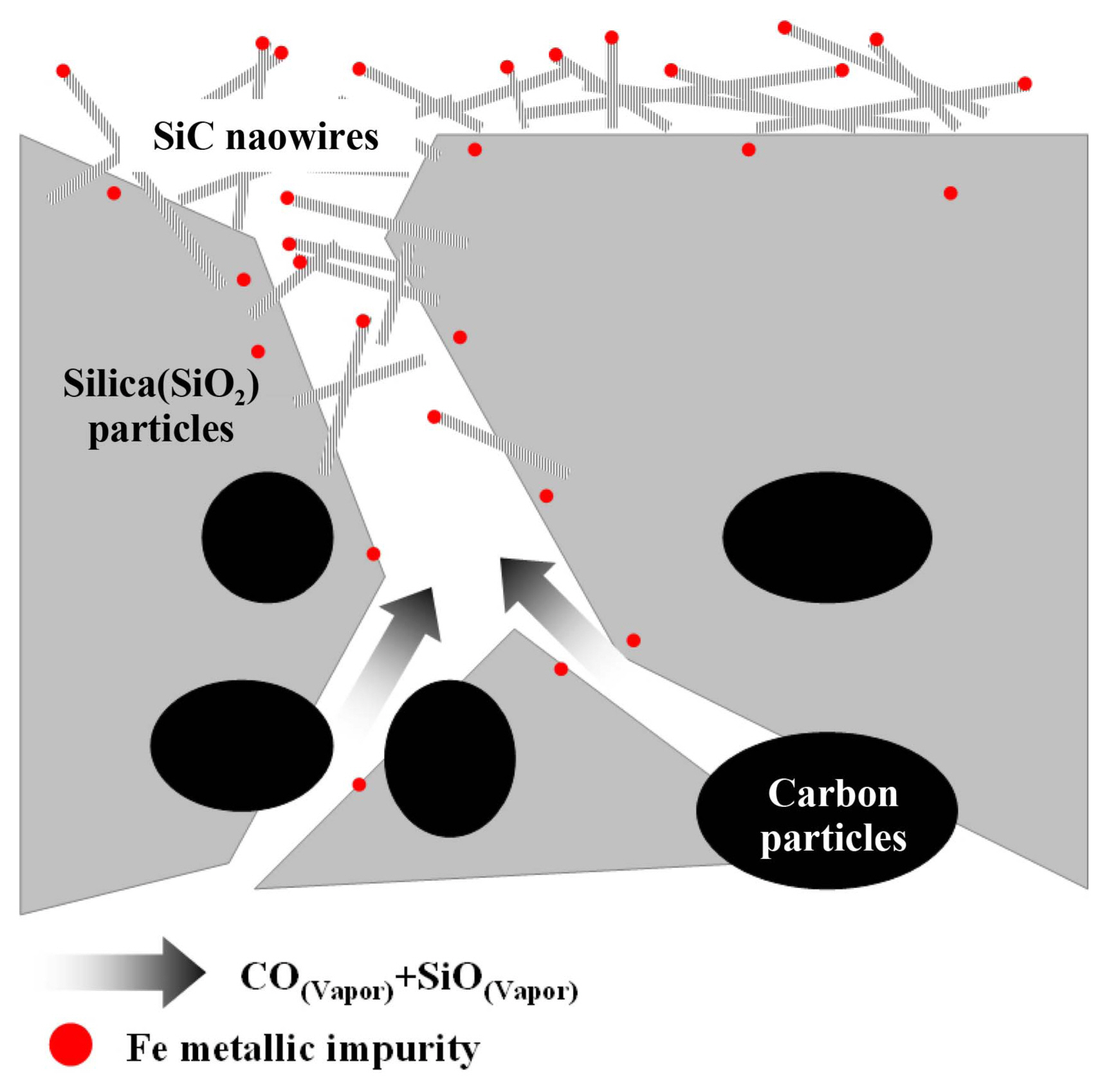
Figure 1 shows a schematic diagram for the growth of PBSiC nanowires by vapor phase reaction through pore channels. During the growth of the PBSiC nanowires, silica and carbon black powder reacted with the evaporating silicon monoxide and carbon monoxide vapor inside the powder surface. At that time, Fe metal catalysts, which were induced by impurities in low-grade silica, diffused out of the surface of the silica particles and formed droplets. Finally, SiC nanowires were synthesized on the surface of the porous body with Fe catalysts acting as nucleation sites.
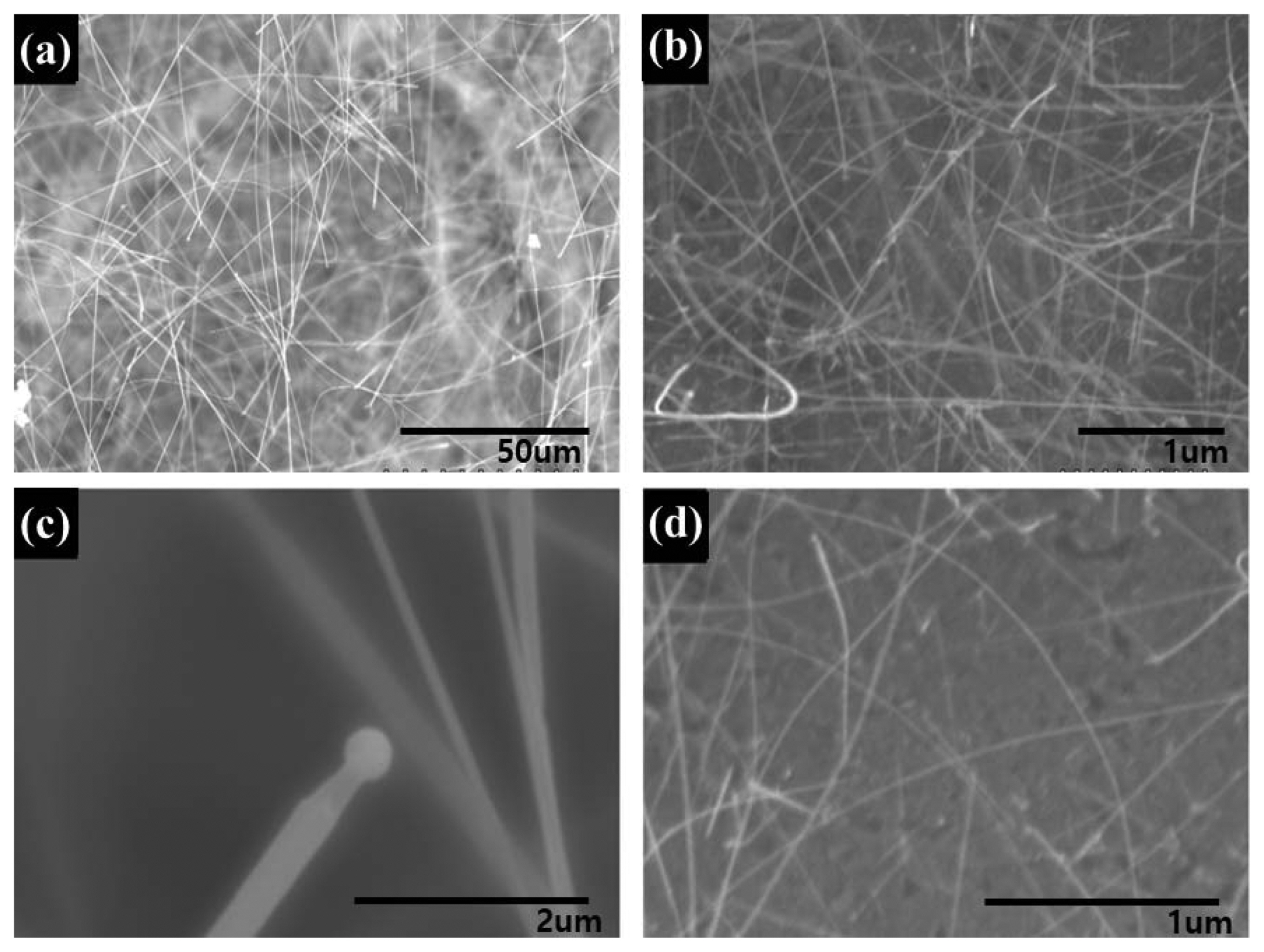
Figure 2 shows the microstructures of PBSiC (Fig. 2(a), (c)) and SWSiC nanowires (Fig. 2(b), (d)) obtained using scanning electron microscopy. All of the as-grown SiC nanowires were prepared at 1400°C temperature for a duration of 1 h. The PBSiC nanowires grown on the surface of the porous body exhibited a wide variation in diameter within the 30 - 400 nm range and a length of over 50 μm. Fig. 2(c) clearly shows a liquid droplet at the end of the nanowire, which typically occurs during VLS growth.14) The SWSiC nanowires grown on silicon wafer ((100) growth plane) were observed to have a relatively uniform diameter of less than 50 nm. The diameter difference in PBSiC nanowires may be due to the silicon monoxide generation rate that depends on the pore size of the porous body. In general, the diameter of the SiC whiskers decreases with increasing silicon monoxide generation rate13) implying that this generation rate is an important process factor in device fabrication. In other applications, it allows for nanowire handling and enables growth of structures with high surface area.
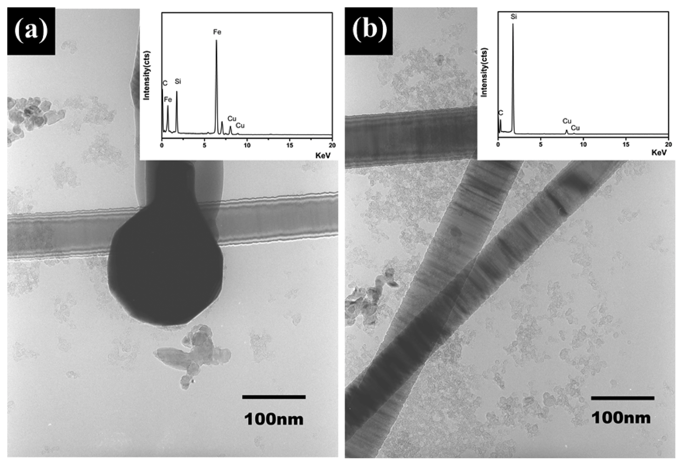
Figure 3 shows low-magnification TEM images and the corresponding EDS spectra (inset images) of the SiC nanowires for impurity analysis. Fig. 3(a) shows the metal tip in the end of the nanowire, which was determined to be Fe. The presence of about 4.25 wt% of various metal impurities such as Fe, Mg, Na, Ca, and K was shown from a formal chemical analysis of silica. Among the impurities, Fe played the role of catalyst in during VLS growth. Fig. 3(b) indicates that inner or outer in the nanowires was not detected other impurity as well as amorphous and oxide layer. Despite the high reaction temperature, the absence of oxides is due to the reduction reaction caused by carbon contained in the raw material.
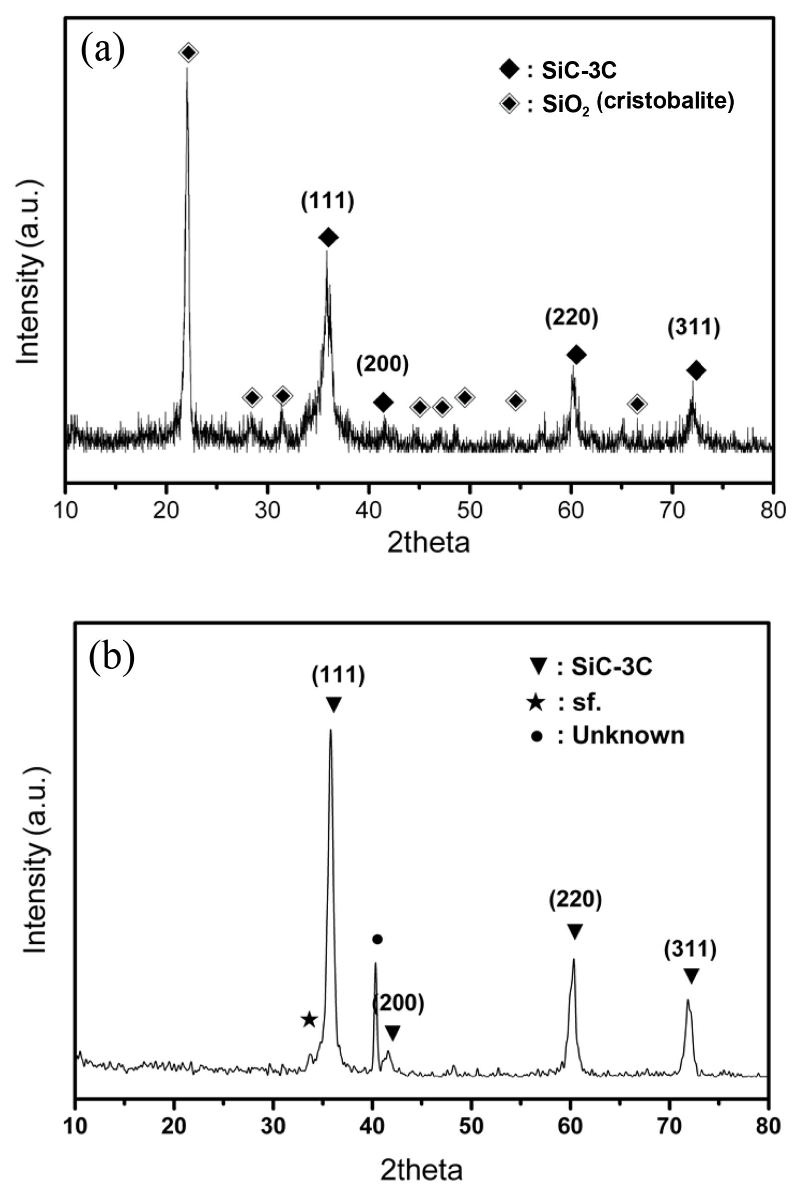
Figure 4 shows the X-ray diffraction patterns of the PBSiC and SWSiC nanowires prepared by the carbothermal reduction process. All the samples could be indexed to a zincblende structure β-SiC (3C-SiC). Fig. 4(a) also shows the presence of another body, which was determined to be silica in a transformed crystalline phase (cristobalite) in the porous body at high temperature. The intensity ratio of the XRD peak at 33.6 and 41.4o I33.6o/I41.4o in the PBSiC and SWSiC nanowires was 0.83 and 1.80, respectively. The intensity ratio increased with increasing stacking fault content.15,16) XRD results confirmed that the stacking fault density of SWSiC was greater than that of PBSiC nanowires.
The HRTEM and SAED (inset in figures) analyses of the PBSiC (Fig. 5(a)) and SWSiC (Fig. 5(b)) nanowires are shown Fig. 5. The SAED patterns of all samples recorded along the [110] zone axis show that the nanowires have cubic zincblende structure with growth along the [111] direction. The bright field image and its analysis establish that the PBSiC nanowire has a smooth surface with 120 nm diameter. No evident stacking faults or twin defects were found in the HRTEM image. No streak was observed in the SAED pattern (see the inset image in Fig. 5(a)) for this sample, which demonstrated that this nanowire has a nearly perfect single crystalline structure. In contrast to the PBSiC nanowire, the SWSiC nanowire was found to have a rough surface and more stacking faults. The SAED pattern of the SWSiC nanowire shows some featureless streaks and spots, which imply that SWSiC has a disorderly layered structure perpendicular to its growth direction.11)
The above results imply that an SWSiC nanowire plays an important role in the formation of stacking faults. It could be explained that the number of stacking faults is related to the nanowire diameter, i.e., the number of stacking faults increases with decreasing nanowire diameter.17) According to the axial next-nearest neighbor Ising (ANNNI) model,18) SiC whiskers with stacking faults have a lower energy than those without stacking faults. Furthermore, the formation of stacking faults promotes [111] facets, which have much lower surface free energy than in other directions, such as [211] or [110]. Therefore, with regards to energetic considerations, the formation of stacking faults during SWSiC nanowire growth is favorable due to the contribution of the stacking faults themselves and the [111] facets at the lateral surface. The specific lateral surface area of the nanowires becomes relatively large when the nanowire diameter is small. This may enhance the formation of stacking faults to reduce the contribution of lateral surface energy.
In addition, the free-standing SWSiC nanowires on silicon substrate allow the effect of stress generated due to the lattice mismatch with the substrate to be excluded. Induced stress acts as a driving force for defect generation. The exclusion of stress effects should contribute to the fabrication of single crystalline SiC nanowires with defects. The result indicates that more stacking faults can also be formed in the SWSiC when the diameter is small and stress is generated by lattice mismatch between the nanowires and the substrate.
4. Conclusions
We report a large-scale synthesis method for SiC nanowires using a porous body and silicon substrate for industrial applications, along with their structural characteristics. SiC nanowires were fabricated from a low-grade silica and carbon black powder using simple carbothermal reduction at high temperature (1300 - 1600°C). PBSiC nanowires with various diameters (30 - 400 nm), long lengths (50 - 200 μm), and high aspect ratios were formed by reaction of silicon monoxide and carbon monoxide through the porous body pore channels. SWSiC nanowires with narrow diameters and more structural defects were synthesized on a silicon substrate at a location near the porous body. All samples were identified as single crystalline β-SiC with growth along the [111] direction. The growth mechanism was discussed in terms of VLS. Chemical analysis of metal tip at the end of the nanowire, as seen in the EDS image, confirmed the role of Fe as a growth catalyst. Fe was induced by impurities in the low-grade silica powder. XRD and HRTEM results confirmed that the SWSiC nanowires contained more defects due to their smaller diameters compared to PBSiC nanowires, which results in a lattice mismatch with the substrate. If the pore size distribution of the porous body can be controlled, it will be possible to synthesize defect-free SiC nanowires with uniform diameter for industrial applications, such as nanowire-enhanced structural ceramics and nanowire-based devices.