


1. Introduction
Many biological organisms have evolved to build three-dimensional (3D) structures with a purpose to utilize the inherent functions, with performances far beyond those of their bulk counterparts.1-4) For example, intricate 3D nanopatterns in the cell walls of diatoms5) and in butterfly wing scales enhance light-matter interactions, acting as photonic crystals for efficient light harvesting or reflection of specific wavelengths.6-8) Inspired by biological systems, different classes of 3D nanostructures have been adopted in photonic, energy harvesting, data storage, and biomedical devices, to exploit their unique electrical, optical, and mechanical properties.9-16)
There has been tremendous effort and progress in the generation of such 3D nanostructures in the past decades; representative approaches include multi-beam interference lithography, photo-polymer waveguide technique, two-photon polymerization, direct 3D writing, polymer phase separation, and various approaches based on printing, molding, and writing.17-21) Despite the advantage of those techniques for achieving artificially well-regulated 3D structures, they are generally limited to producing polymeric structures or some metal or ceramic replica that can be deposited on the polymeric templates at lower temperature. Accordingly, it is difficult to make high-quality and single crystalline 3D structures using those techniques.
In this context, direct epitaxial growth of 3D structures (herein referred to as 3D epitaxy) can be considered as an alternating 3D nanofabrication method. This method is based on the bottom-up approach involving direct growth of inorganic crystal arrays, in which precise position and size control can be achieved in tandem with the top-down strategy.22-27) This feature can also potentially produce a more complex, hierarchically-organized 3D nanostructure through multi-stage epitaxial growth of each crystal constituent, analogous to morphogenesis in biological organizations.
In this review, we provide an overview of our latest progress in 3D epitaxy of oxide and nitride semiconductor crystals, with particular emphasis on the hierarchical organization with position, size, height profile, and 3D organization. Fig. 1 schematically illustrates the basic strategies. We first established a low-temperature, solution-phase epitaxial growth technique to achieve more well-organized and regulated ZnO crystal arrays (Fig. 1(a), left panel). Especially, in tandem with the top-down strategy, the morphology, position, and size control of ZnO crystal arrays can be achieved.28-33) The interactive growth behaviors among the neighboring nanocrystals is also exploited to produce a 3D height profile.34) To further diversify the structures, we also controlled the preferential crystal growth direction by polarity-selective growth behaviors in polar crystals (Fig. 1(a), right).35) Fine tuning of these behaviors during multi-stage growth can especially produce more-complicated 3D nanostructures (Fig. 1(a), center). To expand the applications of this approach, the heteroepitaxial growth of GaN or InGaN multilayers layers on those ZnO crystal templates was established (Fig. 1(b)).36) The critical aspects in the heteroepitaxial growth and its potential application to a 3D optoelectronic device array are addressed.
2. Solution-Phase 3D Epitaxy of ZnO Nanocrystals
2.1. Size and position-controlled growth of ZnO nanocrystal arrays
Crystal growth of ZnO in solution involves a hydrothermal reaction process of zinc ions (Zn2+) and hydroxyl (OH−) ions generated by the dissociation of zinc nitrate and hexamethylenetetramine, respectively. Importantly, the ZnO crystals easily form a vertically-grown 1D nanorod shape, and this anisotropic growth behavior is driven by the crystal structures and surface energy of wurtzite ZnO (Fig. 2(a)). A polar crystal of ZnO is typically composed of O2− and Zn2+ layers in the tetrahedral coordination that are staked iteratively along the c-axis.37) This atomic configuration generally produces a hexagonal rod (h-rod) with a Zn-terminated (positively charged) top (0001) surface and non-polar 6 side (1010) surfaces. In an aqueous solution, OH− groups can easily adsorb on the top Zn2+ layers. The dominant axial growth (i.e., growth along the c-axis orientation) in solution continues by the dehydration reaction of the terminating OH− ion with an OH− ion from the surrounding solution and consecutive capture of positive (Zn2+) and negative (OH−) ions. Previous studies on hydrothermal growth of ZnO crystals showed that ZnO is precipitated from aqueous solution either via direct reaction (Zn2++ 2OH− ⇄ ZnO + H2O) or the hydroxide (Zn2++ 2OH− ⇄ Zn(OH)2 ⇄ ZnO + H2O), depending on the solution conditions. The ZnO growth is involved in Zn(OH)2 intermediate at the high solution concentration, while the growth is performed by direct reaction of precursor ions (i.e., Zn2++ 2OH− → ZnO + H2O) at the low solution concentration.34) Accordingly, position and size-controlled growth of ZnO crystals can be achieved by introducing artificially-defined mask patterns that allow the crystallization reaction to occur only on the (0001) surface of ZnO seed crystals or thin films exposed to the reaction solution (Fig. 2(b)).
In addition to the site-specific crystallization process, morphologies of the resulting ZnO crystals can be controlled by exploiting vertical and in-plane crystallographic orientations of the ZnO seed layers. This effort led to the formation of three types of ZnO 3D nanoarchitectures: (i) flower-like architectures composed of radially-oriented ZnO nanorods on polycrystalline ZnO seed layers with poor c-axis orientation (Fig. 2(c)); (ii) columnar-joint like structures on c-axis oriented polycrystalline ZnO seed layers (Fig. 2(d)); and (iii) h-rod structures with distinctly defined facets on single crystal ZnO seed layers (Fig. 2(e)). Thanks to the strong light guiding in the ZnO crystals, these ZnO nanoarchitectures exhibited increased light extraction and unique light propagation characteristics depending on the nanostructure morphology, which is useful to tailor the emission direction in LEDs and displays.32)
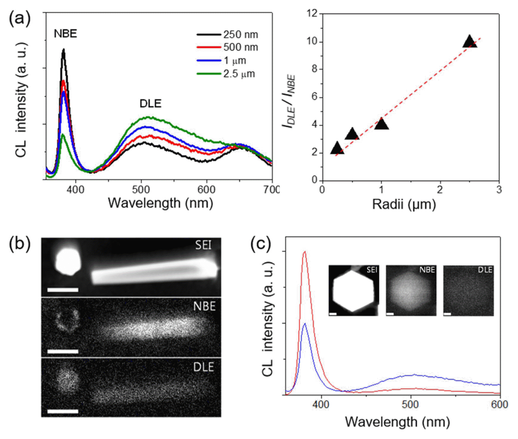
The innovation in the position, size, and shape control of the ZnO h-rods enables the study of surface polarity-dependent luminescent properties, by correlating the size-dependent cathode-luminescence (CL) spectra and spatially-resolved CL microscopy. This is very important given that the surface structure, especially the surface polarity, is associated with surface-related recombination, and its contribution becomes larger at the smaller crystals.38-40) In this effort, it was concluded that the local surface luminescence is closely related to the surface polarities of the ZnO crystals with the following findings (Fig. 3). First, when CL spectra are collected from the top surfaces of ZnO h-rods, the intensity ratio of the deep-level emission to the near-band-edge (NBE) emission peak increased with increasing diameter (Fig. 3(a)). Second, the CL spectral mapping showed an obvious quenching of the band-edge emission on the ZnO top surface (Fig. 3(b)). Given that the positively charged Zn-(0001) surface is generally terminated with OH− ions freely available in aqueous solution, the NBE emission quenching can be associated with the presence of OH− groups. This hypothesis was further supported by the fact that thermal annealing in an oxygen atmosphere prevents emission quenching and leads to bright band-edge emission even on the (0001) surface (Fig. 3(c)).31)
2.2. Engineering 3D height profile of ZnO nanocrystal arrays
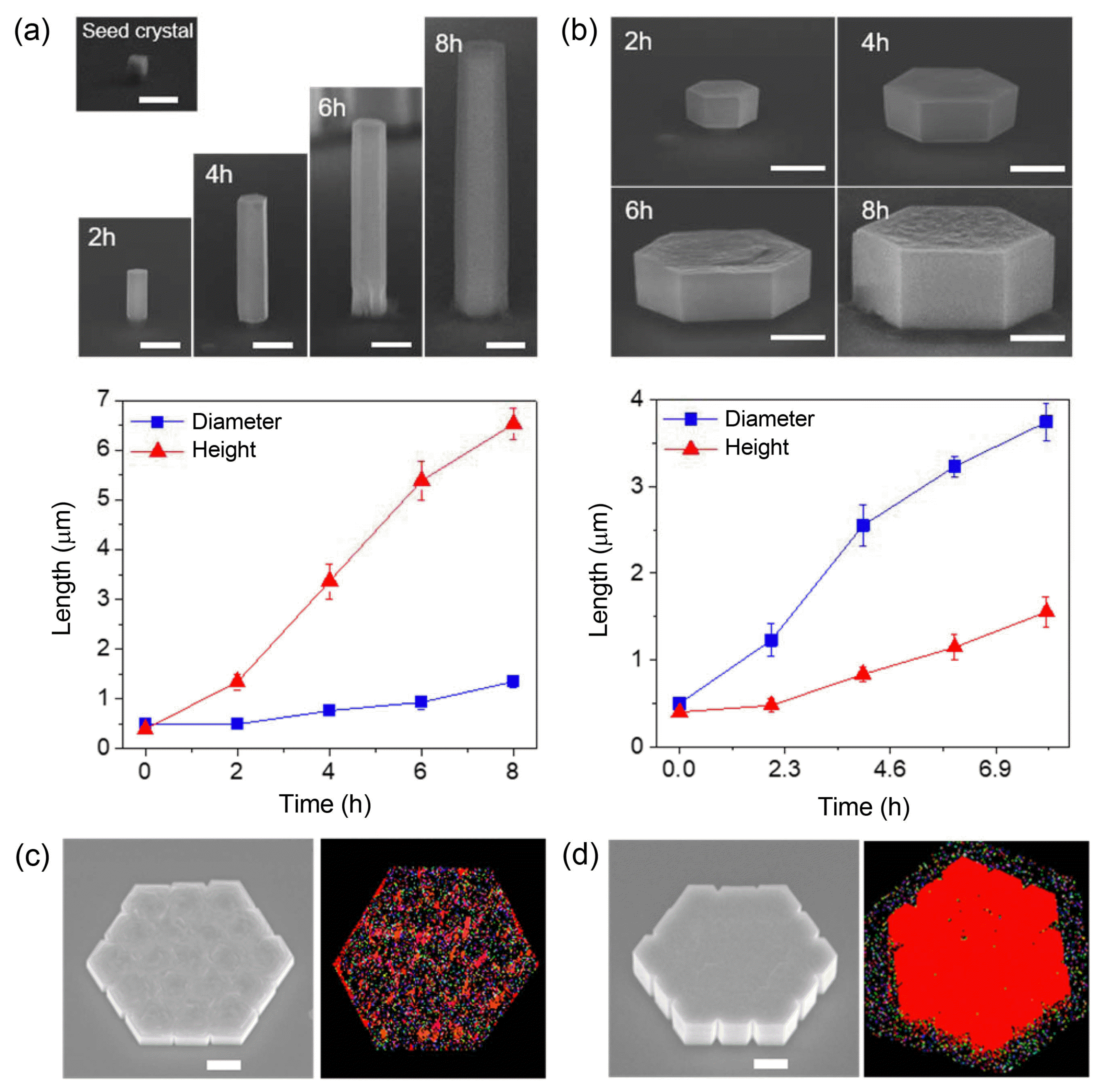
When ZnO rods were grown via PMMA patterns consisting of circular holes with the same diameter on ZnO epitaxial seed layers, their diameter (DZnO) and height (HZnO) were relatively uniform with average standard deviations less than ~ 4% and ~ 2%, respectively. However, the growth of ZnO rods is sensitively affected by solute concentration Cb, which produces three different types of growth regimes characterized by the correlation between DZnO and HZnO: (i) Cb ~ 25 mM, the height is irrelevant to the diameter (Regime I, Fig. 4(a)); (ii) Cb ~ 2.5 mM, the height increases with increasing diameter (Regime II, Fig. 4(b)); and (iii) Cb ~ 1.6 mM, the height decreases with increasing diameter (Regime III, Fig. 4(c)). We also demonstrated that these behaviors could be further exploited to construct sophisticated 3D nanostructures with artificially-regulated height profiles. The systematic investigations and numerical analysis support that these phenomena are attributed to strong interactive growth behaviors, involving the interplays between the Gibbs-Thomson effect, precursor competition, and the synergetic effect.34,41) The characteristic behaviors were employed for ab initio synthesis of specific 3D structures that could not be easily achieved by conventional fabrication methods.34)
2.3. Polarity-controlled epitaxy for lateral/vertical growth directions
In addition to the fine tuning of vertical growth behaviors, the preferential growth direction needs to be controlled to achieve more exquisite structures, targeting more specific shapes. As discussed earlier, vertical growth of ZnO crystals is associated with the positively-charged top surfaces. Accordingly, we can switch the growth direction either towards vertical or lateral by modulating the surface polarity. For instance, if negatively-charged capping agents are added to the reactant solution, the agents would adhere preferentially to the positively-charged top (0001) surface, which then prohibits vertical growth and instead makes the lateral growth dominant.28,42) As a capping agent, a citrate additive (trisodium citrate) was tested. Time-dependent analysis of the diameter and height change without and with a citrate additive revealed that the citrate additive restricts vertical crystal growth and boosts lateral growth so that the relative width to height ratio increased by more than 10 times (Figs. 5(a) and (b)). Nevertheless, the laterally-grown ZnO hexaplates generally have a rough top surface, indicating that the citrate additive may interrupt the epitaxial growth (Fig. 5(b)). This feature was further confirmed by the structural analysis via electron backscatter diffraction (EBSD) and cross-sectional transmission electron microscopy (TEM), which revealed the existence of many tilted domains. This phenomenon is attributed to the interruption of citrate ions for epitaxial stacking of Zn and O ions owing to the charge imbalance between Zn2+ ions and citrate−3 ions. To balance the charge neutrality, NH3+ ions were additionally introduced and their effects on the surface morphology and crystallinity were vigorously investigated.43,44) This study proposed optimal concentrations of citrate and NH4OH additives to achieve nearly single crystalline ZnO hexapla tes with a smooth and flat surface (Figs. 5(c) and (d)). The tuning of the growth direction represents a step advance in 3D epitaxy, enabling precise control of each crystal component and ultimately producing the targeting structures.35)
3. Hetero-Epitaxial Growth of 3D GaN Crystals
3.1. Hetero-epitaxial overgrowth of GaN layers on ZnO crystal array
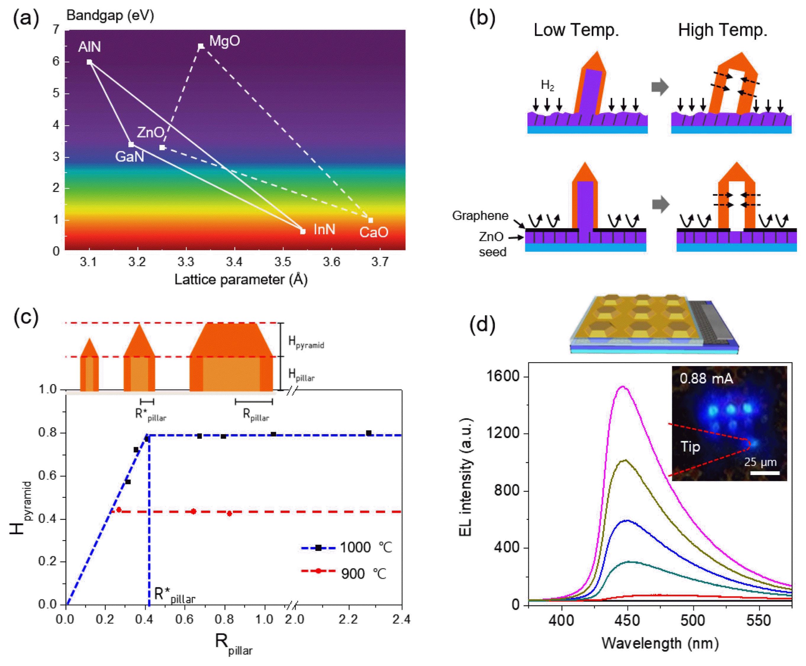
To further apply our strategy to other material systems, overgrowth of different semiconductor layers on the ZnO crystal templates was tested. Since GaN and ZnO have the same wurtzite crystal structure and similar lattice parameters and bandgap, GaN-based semiconductors are considered a strong candidate for heteroepitaxial growth on 3D ZnO crystals (Fig. 6(a)).35,45,46) In particular, compared with planar structures, the 3D GaN/InGaN structures have unique features such as low dislocation density, enhanced light extraction efficiency, and multi-color emission due to varied indium composition and well width in quantum wells.47)
However, direct growth of GaN on the ZnO template is problematic since etching of a ZnO seed layer during high temperature GaN growth in a H2 and NH3 ambient eventually causes the collapse of GaN crystals, as shown in this image (Fig. 6(b), top). To overcome this problem, patterned graphene sheets were employed instead of a resist-based growth mask, given that graphene is an efficient gas barrier material (Fig. 6(b), bottom). In addition to this strategy, the two-step growth of GaN layers on core ZnO crystals enabled vertically-aligned GaN crystal arrays. Interestingly, even when the core ZnO templates were etched away, the remaining GaN crystal arrays stand vertically.36)
3.2. Morphology-controlled growth of a 3D GaN crystal array
This approach was tested on diverse types of ZnO templates, which enabled diverse exterior morphologies of GaN crystals. Systematic investigations revealed that the GaN crystals on ZnO rods have generally sharp tips, producing a pencil-like morphology. With increasing diameter of the crystals, the tip height also increases, but saturates at certain values. For example, for the crystals grown at 900°C and 1000°C, the tip heights saturate at 0.4 μm and 0.8 μm, respectively (Fig. 6(c)). This result can be explained by the interplay of absorption and desorption of Ga adatoms on the top (0001) and side (1-101) planes, which is very sensitive to temperature. The resulting growth behaviors depending on diameter and temperature could be exploited to diversify the exterior morphologies of GaN crystals, such as pencil-, hexagonal-tent-, plate-, and disk-like crystals.36)
3.3. 3D GaN-based micro-LED array
To achieve a p-n junction structure for LEDs, n-type and p-type doped layers were subsequently grown on the GaN cap layers. The cross-sectional TEM image and selected area electron diffraction (SAED) pattern showed that the 3D shaped GaN crystals sustained single crystallinity. The 3D p-n junction GaN crystal array was further employed to fabricate a blue light emitting micro-crystal array by making ohmic contact electrodes to bottom n-type and top p-type GaN layers. Fig. 6 schematically illustrates the micro-LED array (top panel) and blue emission from the 3 × 3 array of the micro-LEDs under forward bias (bottom panel).36) In the case of heteroepitaxial structures consisting of GaN/InGaN single quantum well (SQW) structures, z-contrast scanning TEM (STEM) and energy-dispersive X-ray spectroscopy results confirmed the existence of InGaN SQWs embedded in the GaN wells. Importantly, these analyses showed that both the indium composition and quantum well width change according to the facets as well as the diameter of the crystals. This achievement represents additional opportunities to impose new functions in LEDs, such as multi-color (broadband) emission, wavelength tuning, piezo-photo-electricity, and light extraction or confinement in three dimensions.
4. Conclusions and Outlook
In this review, we provided an overview of the latest progress on the direct synthesis of 3D nanostructures constructed with well-regulated, single crystalline ZnO crystals, and subsequent heteroepitaxial growth of GaN-based multilayers. First, we presented the low-temperature solution-phase synthesis of vertically-aligned ZnO h-rod arrays with well-regulated size, position, and morphology. Second, we highlighted the growth behaviors, focusing on the axial and lateral growth rate correlated to the diameter and interspacing of nanocrystals, as well as the concentration of additional ion additives. Third, the strategy to prevent collapse of the ZnO crystals during hetero-epitaxial overgrowth of GaN layers was introduced. Due to this strategy, the temperature-dependent growth behaviors of GaN crystals on diverse types of ZnO templates could be elucidated, which can facilitate the control of exterior morphologies of resulting GaN crystals, including hexagonal-pencil, hexagonal-tent and plate shapes. We further demonstrated a 3D light emitting crystal array through subsequent growth of high-quality n-type and p-type GaN layers and GaN/InGaN SQW structures. We believe that our fabrication concept of exploiting 3D epitaxy could provide new opportunities towards a multi-pixel array of 3D electronic and photonic systems with new functionalities.