


1. Introduction
1.1. Needs for Photoelectrochemical Water Splitting
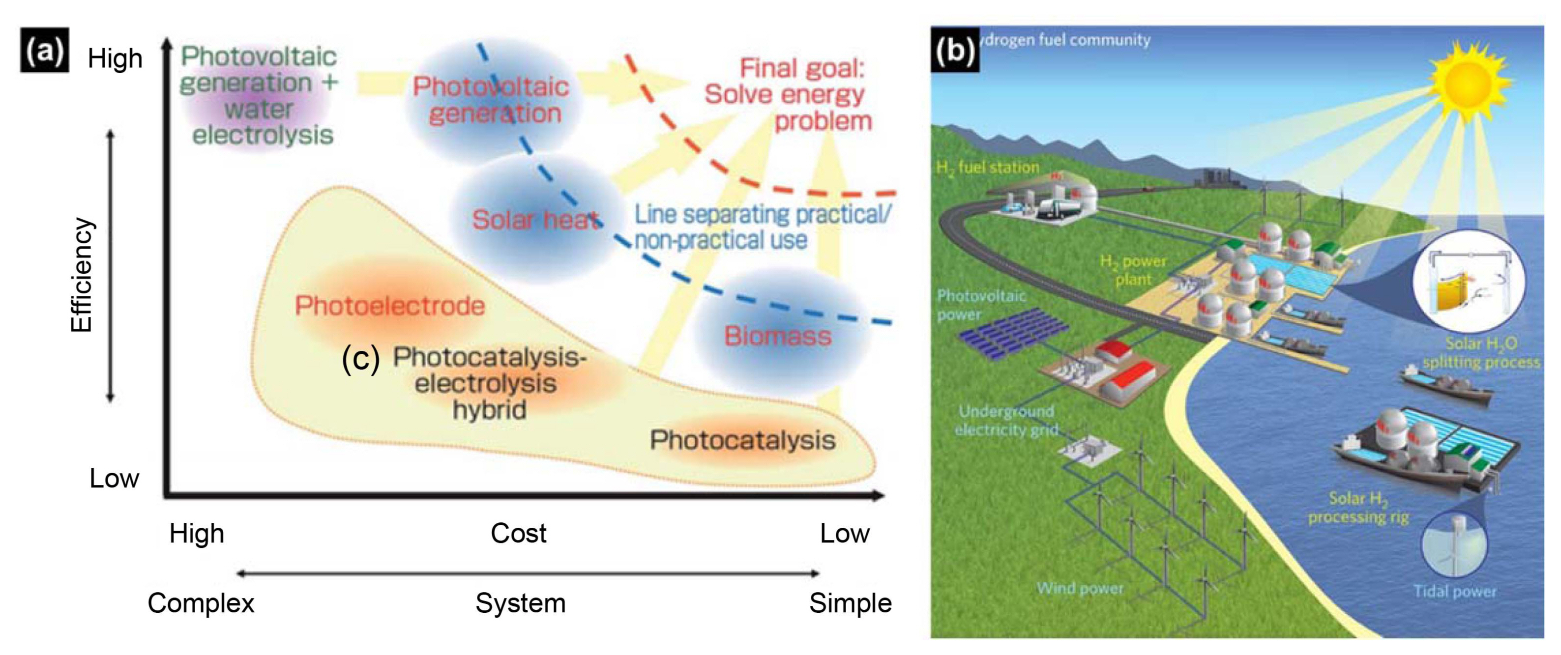
The depletion of conventional fossil fuels, which are insufficient to meet the energy requirements of an increasing population, is of growing concern for the human race and for socially sustainable development.1-6) Thus it is extremely urgent to search for viable alternative renewable energy sources to replace fossil fuels. Renewable energy sources include solar, wind, wave, and biomass, among which solar energy possesses a theoretical potential of 1.2 × 10⁵ TW, more than any other energy source,2) and could in theory easily meet the world’s total energy consumption. Solar electricity produced by photovoltaics is still very expensive, difficult to store for long periods, and challenging to distribute over long distances; hence, the efficient and inexpensive conversion of solar energy into chemical energy such as hydrogen is considered a highly desirable way to satisfy long-term energy needs and cost-effectiveness, as shown in Fig. 1(a) and Table 1.7-8) Among envisioned approaches, as shown in Fig. 1(b), photoelectrochemical (PEC) water splitting has attracted considerable interest for storing solar energy in chemical bonds via generation of hydrogen.3,8-13)
The unit costs of various energy sources, stated in Table 1,7) demonstrate that lowering the energy production cost of PEC water splitting should be treated as an urgent mission for satisfying its cost competitiveness compared with fossil fuel.14) The United States Department of Energy (US-DOE) stated in 2011 that the upper limit cost of hydrogen in 2020, which would make this a feasible fuel, would be 2 - 4 USD per kg.7) The present cost target for hydrogen generation with PEC water splitting, 5.7 USD per kg, must be further reduced to meet the maximum cost suggested by US-DOE. A similar proposal was announced by the Ministry of Economy, Trade and Industry (METI) of Japan in 2008. METI suggested 40 JPY per Nm3, which is of similar value to the US-DOE proposal, as a hydrogen cost target in 2020.7) Table 1,7) put together by Sayama in 2015, shows the unit energy costs of various energy resources including current energy resources and renewable sources with high potential. It can be seen that the unit energy cost of current energy resources are usually below 2 JPY per MJ, and the unit energy costs of renewable energy sources are much more expensive than current energy resources. Even though the cost for fossil fuel seems to be on the rise, a further reduction in renewable energy costs is imperative. This is especially true in the case of hydrogen production by PEC water splitting; according to the analysis of Shaner,15) simply attaining very high solar-to-hydrogen conversion efficiency will not guarantee PEC water splitting technology becoming a cost-competitive energy resource. In this regard, much greater advances in system cost reduction are needed.
Figure 1(b), suggested by Tachibana et al. in 2012,16) demonstrates a design for an artificial photosynthesis plant using available renewable energy such as tide, wind, and solar energy for maintenance cost reduction. It would be possible to implement this kind of facility in any seashore or off-shore location where seawater could be pumped and filtered efficiently. However, in order to fulfill large amounts of energy demand with hydrogen fuels, the implementation of large area PEC cells would also be needed. As stated by Maeda et al.,17) a solar hydrogen plant with PEC cells (solar energy conversion efficiency of 10%) having an area of 25 km2 would produce 570 tons of hydrogen from 5100 tons of water per day. And to supply one-third of the world’s energy requirements in 2050, tens of thousands of hydrogen plants would be needed. To satisfy these demands, scalable, and cost-effective fabrication systems for PEC cells would need to be developed and well-established.18)
1.2. Advantages of Solution Process
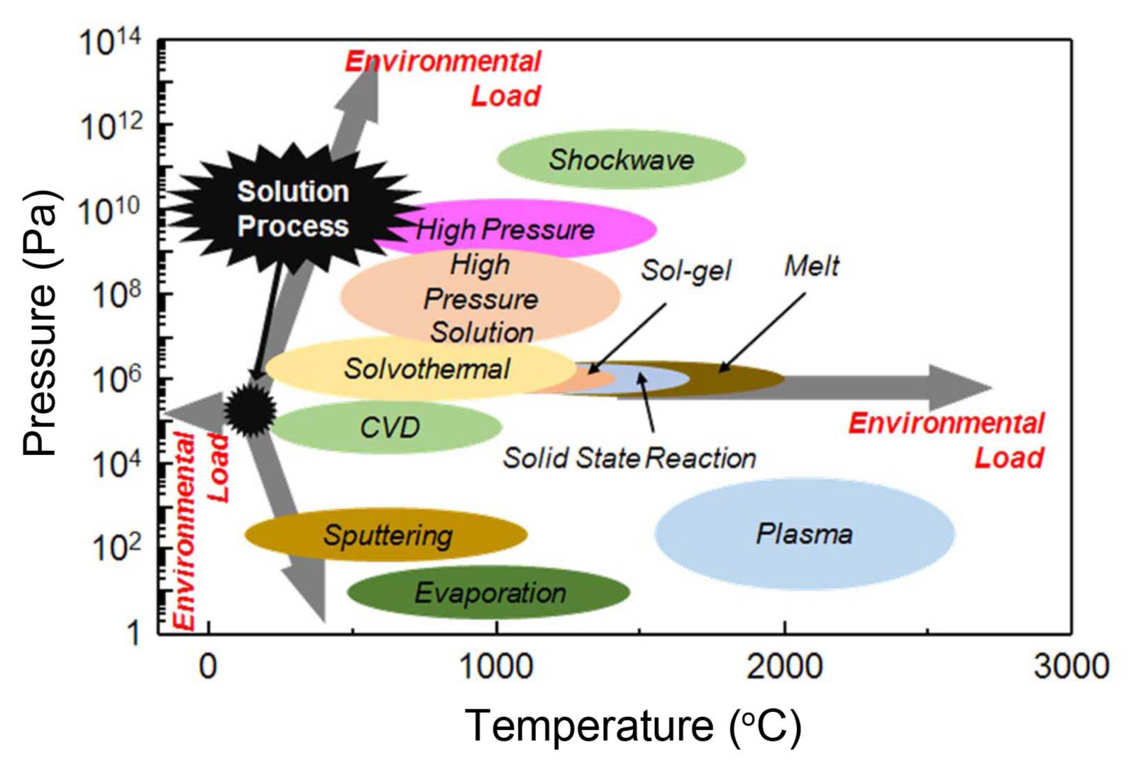
From this point of view, solution fabrication methods, such as hydrothermal and electrophoretic deposition, are attractive in terms of their scalability, financial advantages and eco-friendliness.14,19-24) As displayed in Fig. 2, vacuum processes that are currently widely used for many film fabrication methods aggravate global environmental load. Additionally, not only low-pressure fabrication methods but also high-pressure and high-temperature methods contribute environmental load. Without escaping from these types of fabrication method, it is impossible to avoid worsening the environmental footprint. One of the biggest reasons for replacing fossil fuel with renewable energies is to minimize the additional environmental footprint, which makes the advancement of cost-effective and eco-friendly fabrication methods for PEC cells an urgent challenge. Overall, it is obvious that solution based-fabrication methods are a very promising pathway for PEC cell fabrication.
1.3. Basic Principles of Photoelectrochemical Water Splitting
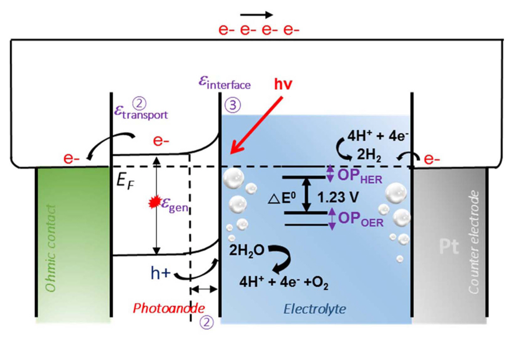
The fundamental principle and critical factors of PEC water splitting are displayed in Fig. 3. The interaction of light with a semiconductor as the photoanode generates electron and hole pairs in the semiconductor. The electrons can be excited from the valence band (VB) to the conduction band (CB) of the semiconductor under irradiation by light of suitable wavelengths, leaving holes in the VB.1-2,8,16,25) These electrons and holes can then transfer to the surface of the photoelectrode and initiate hydrogen and oxygen evolution reaction (HER and OER), respectively. Thus, the position of the CB and VB energy levels of the photoelectrode is crucial to achieve efficient solar water splitting. From a thermodynamic point of view, the minimum of the CB must be located at a more negative potential than the reduction potential of H+ to H2 (0.41 V vs. NHE at pH 7), while the maximum of the VB must exceed the oxidation potential of H2O to O2 (0.82 V vs. NHE).1) In order to drive the water splitting reaction, the photoelectrode must absorb light irradiation to make its electrode potential higher than 1.23 V. In addition, due to energy losses, a kinetic overpotential (OP) is needed to drive the HER and the OER, and thus the band gap energy (Eg) of the semiconductors as photoelectrodes should lie in the range of 1.5 to 3.1 eV, which is within the visible range of the solar spectrum.2) The key criteria for efficient solar water splitting are expressed as the product or the light absorption efficiency; the charge separation efficiency and the injection efficiency of the photogenerated carriers to the reactants; a broad light absorption range; efficient charge transfer from the bulk of the semiconductor to the surface; and rapid consumption of the photogenerated carriers for the surface reaction with minimum overpotential.2,8,26)
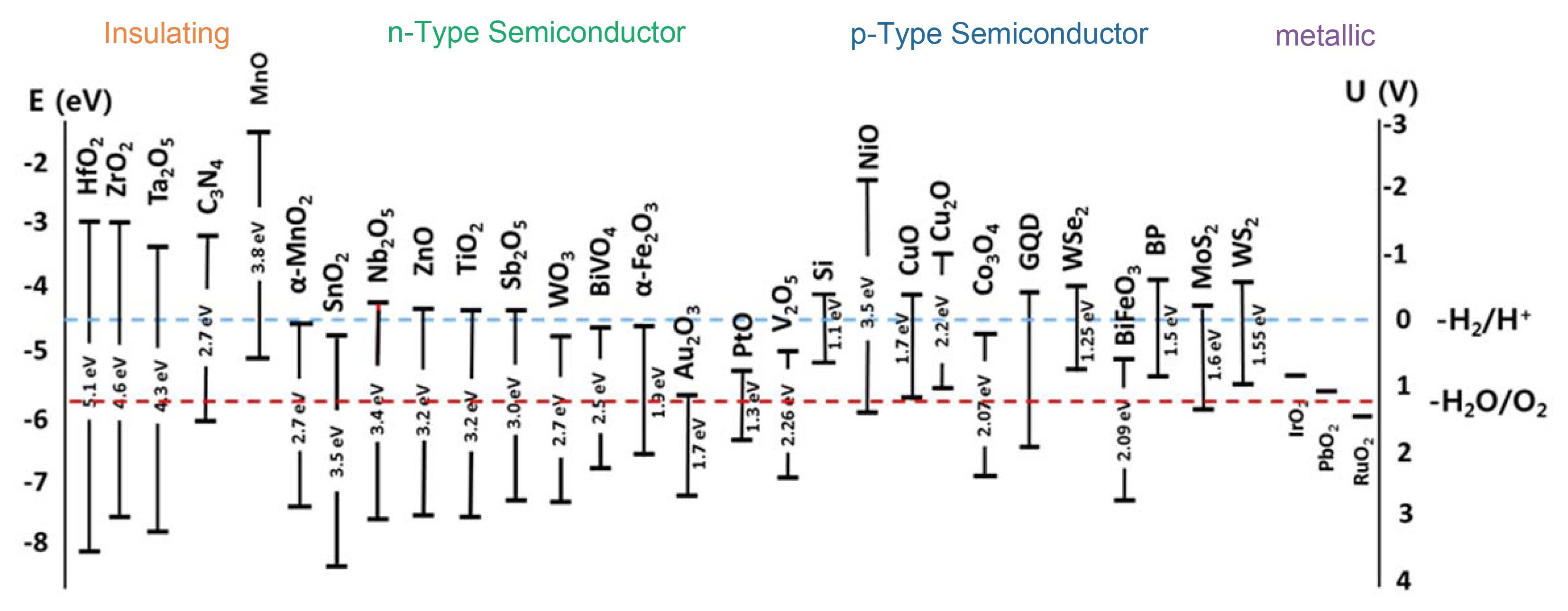
Another critical factor, which may limit the utilization of several photoelectrode materials, is resistance to photocorrosion, or electrochemical stability. Many non-oxide semiconductors show poor stability due to undesired photocorrosion or anodic photodecomposition, while metal oxide semiconductors are usually more stable over a wide range of pH values in aqueous environments upon illumination. Metal oxides attract considerable attention due to their excellent chemical stability, suitable band edge positions, low cost, and tunable bandgaps.1,8,11,27) Metal oxides are usually one of the most stable forms of metal compounds in nature and can be easily synthesized.8,28) Moreover, metal oxides have a wide distribution of band gap and band edge positions, as shown in Fig. 4.
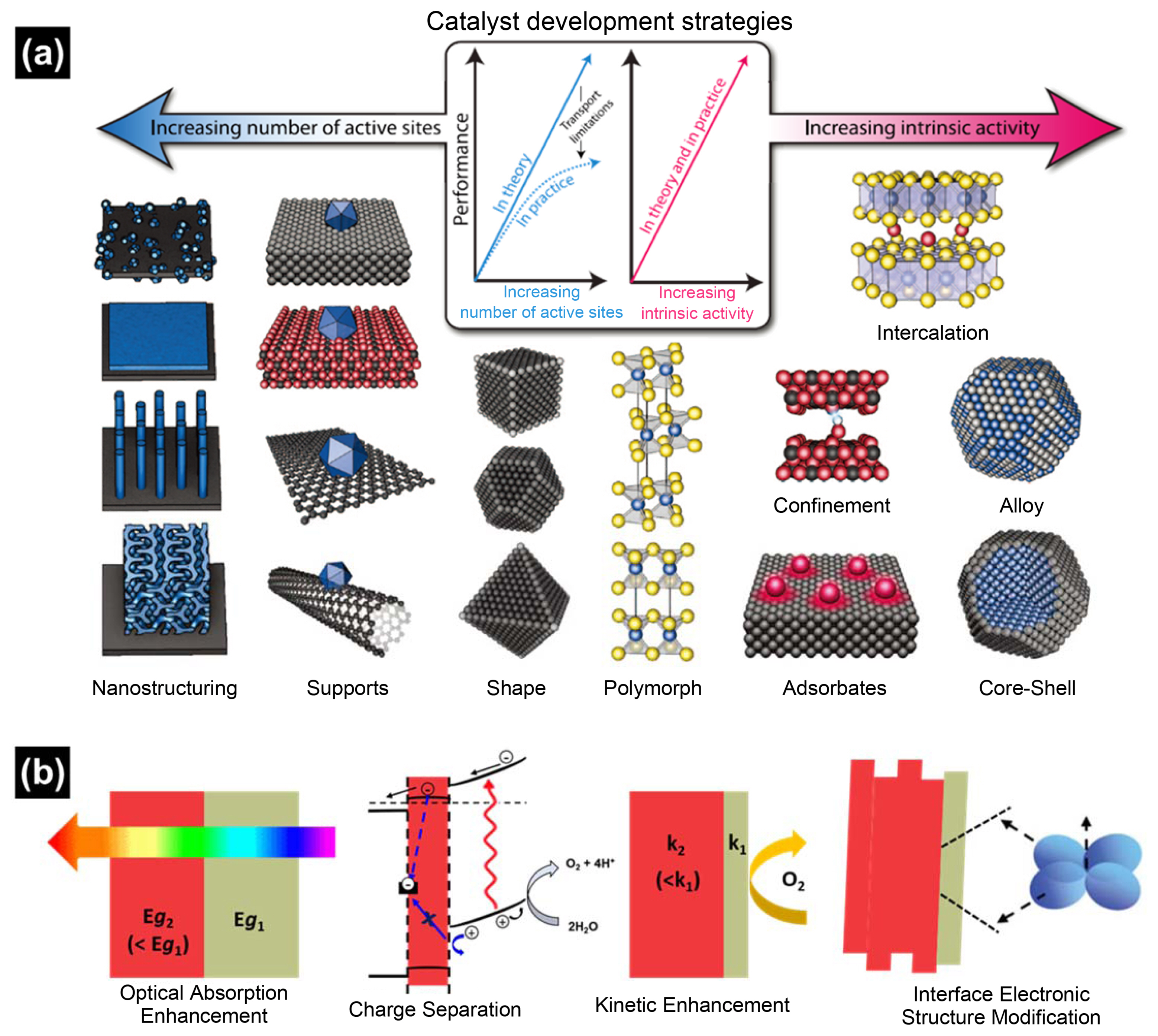
To design highly efficient photoelectrodes for water splitting, all of these typical processes such as light absorption, charge separation, transport, and utilization must be comprehensively considered and optimized. The current bottleneck of photoelectrodes is a lower quantum yield than theoretical values, which is strongly affected by severe electron-hole recombination, sluggish photo-generated carrier transport and extraction, surface back reaction, and poor stability.3,26) So far, the efficiency improvement of photoelectrodes is one of the most challenging tasks in solar water splitting systems for practical use. A variety of strategies such as nanostructuring, heterojunction, and co-catalysts have been developed to address the aforementioned drawbacks of metal oxide photoelectrodes for PEC water splitting, and these are summarized in Fig. 5.29) Most of all, compared to their bulk counterparts, nanostructured materials with smaller size and larger interfacial surface area can effectively shorten the diffusion distance for photo-excited charge carriers and facilitate electron-hole separation at the electrode/electrolyte interface, thus improving charge collection and utilization efficiency.3,10,16) Therefore, in this review, we focus primarily on nanostructured photoelectrodes with outstanding photoactivity.
This review covers the fundamental aspects of PEC water splitting, focusing primarily on nanostructured metal oxide semiconductors synthesized by solution processes. We report on several studies using nanostructured metal oxides as photoelectrodes for PEC water splitting. The limitations of commonly used metal oxide photoanodes and photocathodes for PEC water splitting, as well as the strategies developed to address them, will be thoroughly discussed. Finally, we will provide a brief outlook of the current concepts and future opportunities for metal oxide photoelectrodes in PEC water splitting.
2. Recent Advances in Solution-based Process for Metal Oxide Photoelectrodes
Metal oxides, including Fe2O3, BiVO4, WO3, TiO2, and Cu2O, have been extensively explored for PEC water splitting, since they are usually inexpensive, stable, and easily prepared on a large scale for practical applications. To improve the efficiency of metal oxides as photoelectrodes, elemental doping, pairing with various oxygen evolution catalysts (OECs), heterojunctions, and nanostructuring have been studied. Among these, we will focus primarily on diverse nanostructures of metal oxides for water splitting synthesized by solution processes. Table 2 summarizes recent studies of metal oxide photoelectrodes synthesized by solution processes.
2.1. Photoanodes
2.1.1. Hematite (Fe2O3)
Iron is the fourth most common element in the earth, where it is already oxidized into ferrous (+2) or ferric (+3) states. Among the crystal structures of iron oxide, hematite is the most thermodynamically stable form, i.e. the most commonly founded in nature. In consideration of system costs, the cost of materials for photoelectrodes needs to be treated as a serious requirement. Its electronic properties as an n-type semi-conductor make hematite a potentially promising photoanode material. The energy band gap of hematite is usually reported to be in the range of 1.9 to 2.2 eV, corresponding to 650 to 560 nm of wavelength.30) The absorption of yellow to UV photons that are most abundantly contained in incident photons31) is strong for this reason. Coupled with its earth-abundance, non-toxicity, and stability in aqueous solution, its electronic properties as a semiconductor make hematite an attractive material for artificial photosynthesis. Exploration of hematite as a solar energy conversion material was first carried out by Hardee and Bard in 1976.32) They fabricated hematite thin films on Ti and Pt substrates by chemical vapor deposition. Since that time, continuing studies on hematite have been carried out with various fabrication methods, including solution-based processes.30,33) Herein, only a few notable trials with nanostructured thin films based on solution fabrication methods will be introduced.
Researchers have tried to generate thin films of hematite with donor doping,34-37) as hematite has a short diffusion length (LD = 2-4 nm)37-38) and poor majority carrier conductivity.35,39) An increase of doping concentration in turn reduces the width of a space-charge layer between the photoelectrode and the electrolyte. When assuming classical depletion layer theory,40) only 7 nm width of depletion layer is generated in the case of Nb- doped single crystal hematite with a concentration of 5 × 1019 cm−3.35) However, although dopants were added, the relatively low adsorption coefficient for hematite41,42) straddles carrier separation if hematite has a planar structure. Because the adsorption depth for planar hematite is in the range of 120 - 46 nm for photon wavelengths of 550 - 450 nm,43) fast recombination of excitons will be promoted in the case of a simple planar thin film. Consequently, overcoming these limitations has always been treated as the major barrier for hematite utilization.
In this regard, a recently reported study suggests adaptation of doping and nanostructuring simultaneously. Sivula et al.44) reported mesoporous hematite thin films on fluorine-doped tin oxide (FTO) substrate prepared by a solution-based colloidal method. For preparation of the precursor paste, a solution was synthesized by combining 400 mg of Fe2O3 nanopowder, with 40 μL of a 10% solution of acetylacetone (Acac) and 1-hexanol using a mortar and pestle. The prepared solution was diluted with 1% Acac in 2-propanol, and this was well-dispersed in a water-bath (10°C) by an ultrasonic tip sonicator. Finally, the dispersed solution was concentrated by evaporation and mixed with a 4 wt% solution of hydroxypropyl cellulose (HPC) in 2-propanol. The prepared precursor paste was coated on FTO substrate by doctor-blade at a thickness of 40 μm, and then annealed by a two-step process in order to remove the organics. Prior to reaching the set point (700 - 800°C), an initial heat treatment was carried out at 400°C for 10 h. Fig. 6(a), (b) shows different particle sizes of hematite with respect to the heat treatment temperature. Even though a specimen prepared at 800°C has larger particle size than at 700°C, a much higher photocurrent density was exhibited by the 800°C specimen. Analysis by XPS (X-ray photoelectron spectroscopy) and UV-Visabsorption spectroscopy showed that doping of Sn from the FTO substrate occurs, due to the high thermal energy which induces large effects on optical properties and photoactivity. Souza et al.45) also tested the effect of doping and nanostructure simultaneously by fabricating nanostructured hematite thin films using a polymeric precursor spin coating method. Both nanostructure and silicon doping concentration were controlled by the concentration of tetraethyl orthosilicate (TEOS), which has the role of silicon precursor. For the polymeric precursor, iron(III) nitrate 9-hydrate and TEOS dissolved in isopropyl alcohol were stirred in citric acid dissolved in DI water and heated in the range of 70 - 90°C. Promotion of citrate polymerization was done by stirring and heating after adding ethylene glycol to this solution. Although an optimally-controlled doping concentration of Si exhibited enhanced photocurrent density, it could be seen that the effect of Si doping shows much lower impact compared with Sn doping. For this reason, the effect of doping in hematite relies on the proper type of dopant and enough thermal energy. However, enough thermal energy promotes further growth of crystal size, which highlights the short diffusion length of hematite.
Brillet et al.46) conquered this phenomenon by encapsulation with silica, whose role is to confine further growth of the hematite crystals. The experimental procedure for preparation of precursor paste was very similar to Sivula et al.,45) but titanium isopropoxide was also added for Ti ion doping when the solution was mixed with HPC. First, heat treatment was applied, to remove organic compounds. The encapsulation was then performed by chemical bath deposition. The annealed mesoporous hematite thin films were immersed at 0°C in aqueous methanol solution, hexadecyl-trimethylammonium chloride, and aqueous ammonia in sequence. The encapsulated hematite films were then annealed at 800°C in air. After heat treatment, the silica layer was etched by dilute aqueous NaOH (5 M). Brillet et al. demonstrated an adequate fabrication method to restrict further growth of particle size and an enhancement of the doping effect at high temperature.46)
Deposition of an FeOOH (oxygen evolution co-catalyst) overlayer on hematite was recently tested by Kim et al. for further enhancement of the PEC performance.47) Mesoporous hematite thin films were prepared by simply immersing a FTO substrate in a solution containing 0.15 M FeCl3·6H2O and placing it in an oven at 100°C for 6 h. Fig. 6(f) shows the finely coated FeOOH layer. Prepared thin films were annealed via a two-step heat treatment: 550°C for 1 h followed by 20 min annealing at 800°C. The FeOOH overlayer was deposited by simply immersing hematite thin films into an aqueous solution containing 0.15 M FeCl3·6H2O and 1 M NaNO3 at 100°C for 5 min. An increase in surface reaction can be captured by a decrease of onset potential and a doubling of photocurrent density.
2.1.2. Bismuth Vanadate (BiVO4)
Among oxide photoelectrode candidates, BiVO4 has been identified as one of the most promising n-type semiconductor photoanodes for use in solar water oxidation, since it can absorb a substantial portion of the visible spectrum due to its relatively narrow band gap energy (~ 2.4 eV), and it has a favorable portion of the conduction band very near the thermodynamic hydrogen evolution potential.3,5,8-9,48) However, inefficient charge transport and interfacial charge transfer properties are the key limiting factors for BiVO4 photoanodes.3-4,8,48) The presence of a porous nanostructure in the photoelectrodes provides an increased interfacial area between the electrolyte and the film. The formation of nanostructures enables improvement of the water-splitting efficiency, as the photogenerated holes will have to traverse less bulk material to be collected at the solution interface; therefore it has a lower chance of recombining before participating in the electrochemical reaction.4,27,49) However, increasing the surface area by introducing porosity can also have adverse effects on charge separation and transport, as it can result in an increase in surface states, defect sites, and grain boundaries while decreasing crystallinity. Therefore, the morphologies and surface areas of a photoelectrode should be finely optimized to maximize the overall net positive effect.27)
One interesting study by Xi et al.50) reports that BiVO4 nanoplates synthesized by a hydrothermal method have monoclinic scheelite structures with well-defined facets exposed at the surface. They compared photoactivities of BiVO4 with different morphologies such as nanorods and nanoplates. The BiVO4 nanoplates showed higher photocurrent density than nanorods due to active surface structures of the BiVO4 nanoplates. This study indicates that designing nanostructures with appropriate surface facets is a feasible approach for the improvement of photoactivity.
BiVO4 has also been prepared by a new cathodic electrode-position method, as demonstrated by McDonald, Choi et al.51-52) A polycrystalline BiOI electrode, composed of extremely thin 2D plates, allowed for the preparation of porous BiVO4 photoanodes using a simple chemical and thermal treatment. The resulting BiVO4 with high porosity showed outstanding PEC efficiency. On the basis of these results, Kim and Choi48) modified a previous synthesis developed by McDonald and Choi.51) It is possible to facilitate the production of nanoporous BiVO4, as displayed in Fig. 7(a)-(f), which is composed of much smaller particles, achieving an enlarged surface area.48) The major change was the solution used as the source for conversion of BiOI to BiVO4. They observed that the surface of BiOI film is highly hydrophobic; thus the aqueous vanadium solution used in the study by McDonald and Choi could not easily penetrate into the BiVO4 films. As a result, the conversion of BiOI to BiVO4 was initiated only at the top of the film surface, and the grains of BiVO4 grew toward the bottom of the film by slow solid-state diffusion, resulting in the formation of large particles of BiVO4 and no porosity in that direction, limiting the surface area. When the aqueous vanadium solution was replaced by a more hydrophobic DMSO solution containing vanadyl acetylacetonate as the vanadium source, the solution could easily penetrate the entire BiOI film. Therefore, upon heating, multiple nuclei could form, even within a single BiOI sheet, resulting in the formation of smaller particles, which considerably increased the porosity and the surface area. This research proposed a novel technique of electrochemical deposition and demonstrated that nanoporous morphology with high surface area effectively suppresses carrier recombination without additional doping.
Another approach to improve absorbance and charge separation efficiency of BiVO4 is shown in Fig. 7(g)-(u). Lee et al.5) first introduced shape-controlled gold nanoparticles (Au NPs) as plasmonic NPs on BiVO4 thin film synthesized by pulsed electrodeposition. They reported shape-controlled Au NPs with optimum coverage that significantly promote the photoactivity of BiVO4 in over-band gap photon energy, rather than sub-band gap photon energy. Well-defined octahedral Au NPs significantly increased photocurrent density of BiVO4 about 3-fold, while hemispherical Au NPs reduced it, since largely-enhanced localized surface plasmon resonance electric fields (LSPR-EFs) are only observed with octahedral Au NPs. Finite-domain time-difference (FDTD) simulation also validated intensified LSPR-EFs in the entire UV-vis region from octahedral Au NPs, compared to hemispherical Au NPs, indicating that control of the shape of plasmonic Au NPs is the key to achieving high PEC efficiency.
2.1.3. Tungsten oxide (WO3)
In addition to homogeneous BiVO4, the formation of type II heterojunctions has proven to be effective to facilitate the separation of photo-induced electron-hole pairs, enlarge the interfacial area, and maximize light absorption.3) The combination of BiVO4 and WO3 to form a type II heterojunction not only facilitates charge separation, but also expands the light absorption capability of the composite photoelectrode.3,11,26)
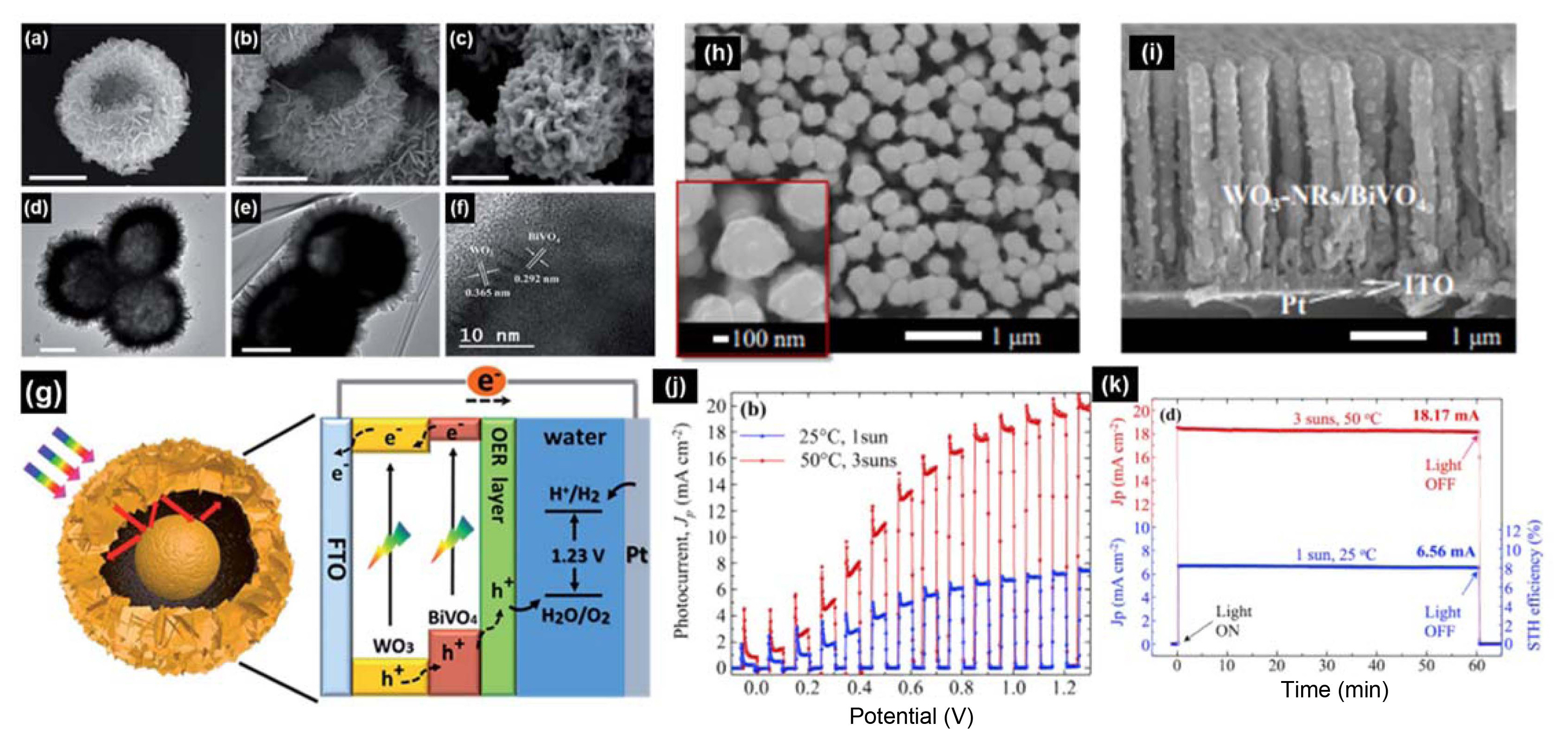
Jin et al. first designed a WO3 thin film consisting of yolk-shell structured nanoparticles via a solution process without the use of vacuum deposition, as shown in Fig. 8(a)-(f).53) A thin BiVO4 layer with a smaller band gap was coated onto the surface of and inside the WO3 shells, providing a rationally-designed inner space between the particles and the shell for better electrolyte accessibility. The yolk-shell-shaped PEC photoanode not only induces efficient light absorption but also plays an important role in electron collection from BiVO4 due to an enlarged contact area. The photocurrent density of the yolk-shell (Y-WO3/BiVO4/OER) photoanode achieved its highest value of 5.0 mA/cm2 at 1.23 V vs. RHE.
Lee et al.3) reported highly ordered one-dimensional WO3 nanorods by changing their porosity and aspect ratio, and depositing stoichiometric BiVO4 on the surface of the WO3 nanorods by pulsed electrodeposition. The notable point of this research is that cross-sectional transmission electron microscopy shows dot-like BiVO4 well coated on the entire surface of the WO3 nanorods. BiVO4/WO3 type II heterojunction anodes can lead to a high photocurrent density of 4.55 mA/cm2 and an incident photon-to-current conversion efficiency of 80% at 1.23 V versus a reversible hydrogen electrode without additional catalyst.
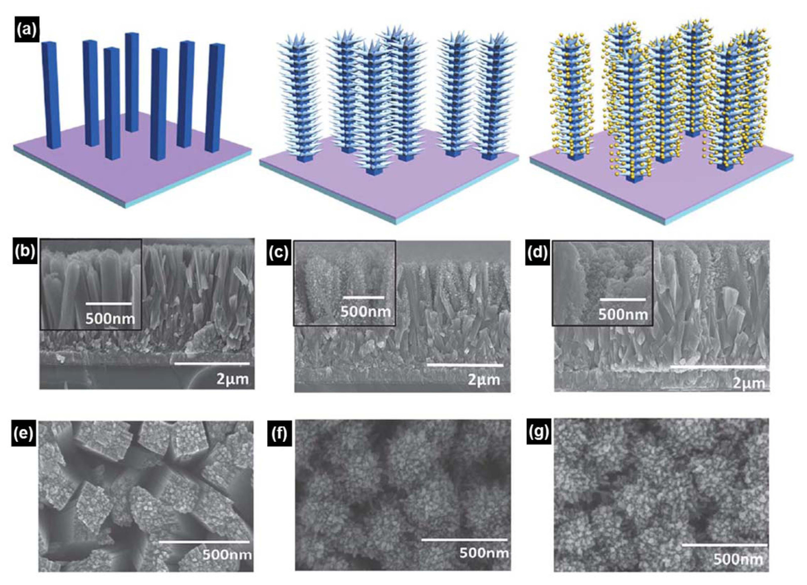
Pihosh et al.54) demonstrated this concept with a WO3/BiVO4+CoPi core-shell nanostructured photoanode that achieves near theoretical water splitting efficiency, as shown in Fig. 8(h)-(k). This study combines BiVO4 with more conductive WO3 nanorods in the form of a core-shell heterojunction, where the BiVO4 absorber layer is thinner than the carrier diffusion length, while its optical thickness is re-established by light trapping in high aspect ratio nanostructures. Their photoanode demonstrates an ultimate water splitting photocurrent of 6.72 mA/cm2 under 1 sun illumination at 1.23 V vs. RHE, which corresponds to ~ 90% of the theoretically possible value for BiVO4.
2.1.4. Titanium dioxide (TiO2)
Titanium dioxide (TiO2) has been favored in many industrial fields for its excellent thermodynamic stability and chemical resistance.55-59) In the case of photocatalytic applications, the discovery of photocatalytic phenomena of TiO2 by Fujishima and Honda in 197260) demonstrated the potential for new applicable areas, i.e. photovoltaics and photocatalysts. Since then, considerable efforts have been made to make TiO2 a promising material for photocatalysis,55,61-65) and today TiO2 is considered one of the potential candidates to play an important role in solving environmental and pollution problems as a photocatalyst. Following the innovative work of Fujishima and Honda, several synthetic methods including sol-gel,66-70) chemical vapor deposition,71-74) physical vapor deposition,75-77) and others78-81) have been adapted to synthesize TiO2 photocatalysts. But most of these cases show a lower photocurrent density than other photoanodes because of a higher resistance and larger band gap (3.0 - 3.2 eV) for TiO2.82) Consequently, these disadvantages would need to be overcome in order to fabricate stable and efficient TiO2 photoanodes. Several strategies have been proposed to maximize the potential of TiO2 as a photoanode, and these will be further discussed here.
One approach to overcome the limit of TiO2 photocatalysts is reinforcement of photon absorption and reaction with electrolytes by increasing surface area to volume ratio,83) and formation of nanostructure is always a good choice to maximize the surface area of films. Some researchers have synthesized TiO2 nanostructure arrays by coating on different nanostructured templates such as anodic alumina membrane (AAM) and ZnO.
In 2003, Lin et al.84) fabricated TiO2 nanowire arrays by electrophoretic deposition into the pores of an AAM. Colloidal suspensions for electrophoretic deposition of TiO2 were synthesized by dissolving titanium tetraisopropoxide (TTIP) in ethanol and mixing with glacial acetic acid solution and the addition of nitric acid to adjust the pH to 2 - 3. An AAM with an Au substrate attached to Cu foil was used as a cathode, and platinum was used as an anode. The deposition condition for the TiO2 coating into the pores of the AAM was a voltage of 2 - 5 V and fabricated films were annealed at 500°C for 24 h. Isolated TiO2 nanowires could be obtained after dissolving the AAM templates in a 5 wt% NaOH solution. The length of the nanowires was dependent on the length of the AAM pores.
TiO2 nanotubes can be fabricated using the sol-gel method and AAM templates. Lee et al. in 200485) dipped an AAM template into a TTIP solution prepared by mixing TTIP with 2-propanol and 2,4-pentanedione, and the sol-coated template was placed under vacuum until the entire volume of the solution was pulled through the AAM. The AAM was hydrolyzed by water vapor over HCl solution for 24 h, air-dried at room temperature, and then calcined at 400°C for 2 h and cooled to room temperature at a cooling rate of 2°C/h. Pure TiO2 nanotubes were obtained after the AAM was dissolved in 6 M NaOH for several min. TiO2 nanotubes could also be obtained by a chemical bath deposition method using AAM. Reported by Liu et al.,86) TiO2 nanotubes could be synthesized by simply submerging AAM template in dilute TiF4 at pH 2.1 and 60°C for 12 - 48 h.
Not only AAM, but also a ZnO nanorod array on glass substrate could be used as a TiO2 nanotube template. Similarly, TiO2 nanotube arrays could be obtained by etching ZnO in a ZnO nanorod template coated with TiO2 by a dip-coating method.87) Dilute HCl was used as an etchant for the ZnO nanorods and, due to the structure of the ZnO building unit, the TiO2 nanotubes had pores with a hexagonal shape.
In order to make TiO2 films as photoelectrodes, it is necessary to generate a junction with a conductive substrate. However, a difference of refractive index between TiO2 and the substrate induces a reflection of incident light which reduces light absorption.88) To overcome this phenomenon, some researchers adapted the characteristics of a rutile TiO2 growth unit. As the crystal planes of TiO2 have quite different surface energies, rutile TiO2 shows preferential crystal growth when synthesized by a hydrothermal process.56,89-91) Using this method, fabrication of a branched nanorod structure has been tried. Cho et al.92) fabricated branched nanorod TiO2 films on a FTO substrate by a two-step synthesis. First, TiO2 nanorods were grown hydrothermally on TiO2-coated FTO substrate. Tetrabutyl titanate (TBT), 25 mL of deionized (DI) water, and 25 mL of concentrated HCl were stirred to create a hydrothermal solution. The obtained TiO2 nanorods films were annealed at 450°C for 1 h in air, and seed nanoparticles for TiO2 branches were deposited by a dip-coating method using the TiO2 polymeric solution. The seeded nanorods films were immersed in an aqueous solution consisting of 10 mL of DI water, 0 - 0.5 mL of HCl, and 0.1 mL of TiCl3 solution and kept at 80°C for 1 - 2 h. Finally, branched nanorod films were obtained by washing with ethanol and annealing at 450°C for 1 h in air. The obtained nanorods and branched nanorods showed much lower reflectance in the UV region compared with porous nanoparticles because of a change in film density from bottom to top and scattering of incident light.88)
Such examples for controlling TiO2 nanostructure have contributed to enormous advances over simple planar thin films, but still further enhancements are needed before TiO2 photoanodes can be commercialized. Based on the belief that research on single TiO2 structures has reached its theoretical upper limit, co-catalyst attached TiO2 photoanodes have been examined recently. Among these, the Au nanoparticle-coated TiO2 branched nanorod structure, reported by Su et al.,93) shows outstanding results. A schematic of the experimental procedure for preparing these nanorods is illustrated in Fig. 9. Similar to the above case, TiO2 nanorods were hydrothermally synthesized on FTO with a solution composed of 30 mL of DI water, 30 mL of concentrated HCl, 1 mL of TBT and 5 mL of 5 M NaCl. Hydrothermally prepared TiO2 nanorods were immersed in 0.2 M TiCl4 at room temperature for 18 h and then rinsed with absolute ethanol. Specimens were annealed at 450°C for 30 min. The fabricated TiO2 branched nanorods were immersed in 0.3 mM HAuCl4, dispersed in DI water, and irradiated with a 300 W Xe lamp for 6 h to coat Au nanoparticles on TiO2 surfaces. The much higher photocurrent density shown in this study demonstrates that both strategies, i.e. increasing surface area and enhancing surface reaction by a co-catalyst, can be successfully adopted at the same time.
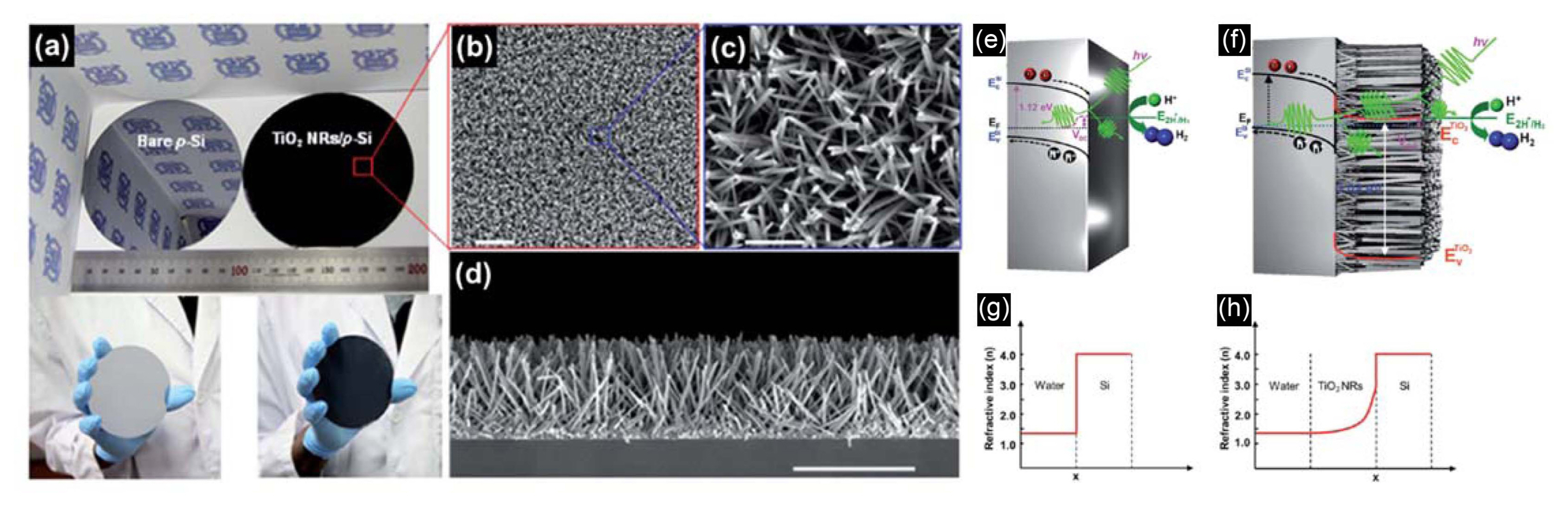
Recently it has been shown that the use of TiO2 can be extended to photocathodes as well as photoanodes. Andoshe et al.88) fabricated a photocathode with a heterojunction of p-Si and TiO2 nanorod thin film. For the heterogeneous nucleation of TiO2 nanorods during hydrothermal synthesis, a 5 nm thick seed layer of the TiO2 film was deposited on p-Si. Subsequently, TiO2 nanorods were hydrothermally grown on a seed layer of deposited p-Si substrate at 180 - 220°C for 0.5 - 2 h. The solution for the hydrothermal process contained 25 mL of DI water, 25 mL of concentrated HCl and 0.8 mL of TBT. As shown in Fig. 10(a), the TiO2 nanorod/p-Si photocathode exhibits a matt black color. As illustrated in Fig. 10(b)-(h), a gradual change in nanorod density along the vertical direction causes a steady change of refractive index that restricts total reflection. TiO2 has the additional role of passivating p-Si from corrosion. Likewise, TiO2 exhibits a potential for heterojunction, passivation, and interface modulation materials.
2.2. Photocathodes
Despite significant efforts over the past decades to develop new photocathode materials for solar hydrogen production via water splitting, there are only a few metal oxide based photocathodes, such as copper-based oxides, that can meet the requirements for commercially viable solar water splitting.8,94-95) Two long-standing bottlenecks for metal oxide photocathodes are sensitivity to photocorrosion during the hydrogen production process and low quantum efficiencies. Here, we review recent developments using metal oxide-based photocathodes synthesized by a solution process for efficient and stable water splitting.
2.2.1. Cuprous oxide (Cu2O) and Copper oxide (CuO)
Cu2O and CuO are the most representative p-type binary oxides that have been introduced for use in solar water splitting. In addition to their favorable band gap energies that allow for the utilization of visible light, the low cost, earth abundance, and non-toxicity of Cu are additional advantages for developing Cu-based photoelectrodes.94)
Cu2O, with a direct band gap of 2.0 eV, is an attractive oxide for solar water reduction, thus it is possible to theoretically reach a photocurrent of 14.7 mA/cm2 and a solar to hydrogen efficiency of 18%. The major limitation of Cu2O is photocorrosion (e.g., Cu2O + 2H+ + 2e− → 2Cu + H2O).96) Paracchino et al.97) successfully synthesized Cu2O films by using electrochemical deposition, which was produced by cathodic reduction of Cu2+ ions in an aqueous alkaline (pH 12) solution. Cu2O grains were covered with metal oxide protective layers [5 × (4 nm ZnO/0.17 nm Al2O3)/11 nm TiO2] via atomic layer deposition (ALD), and finally coated with Pt nanoparticles, resulting in outstanding film quality when coated by ALD. Significantly, the protected Cu2O photocathode exhibited substantially improved photoactivity and stability. The surface-protected Cu2O achieved a photocurrent density of − 7.6 mA cm−2 under AM 1.5 illumination; furthermore, the protected electrodes remained photoactive after 1 h of testing and the measured Faradaic efficiency was close to 100%.
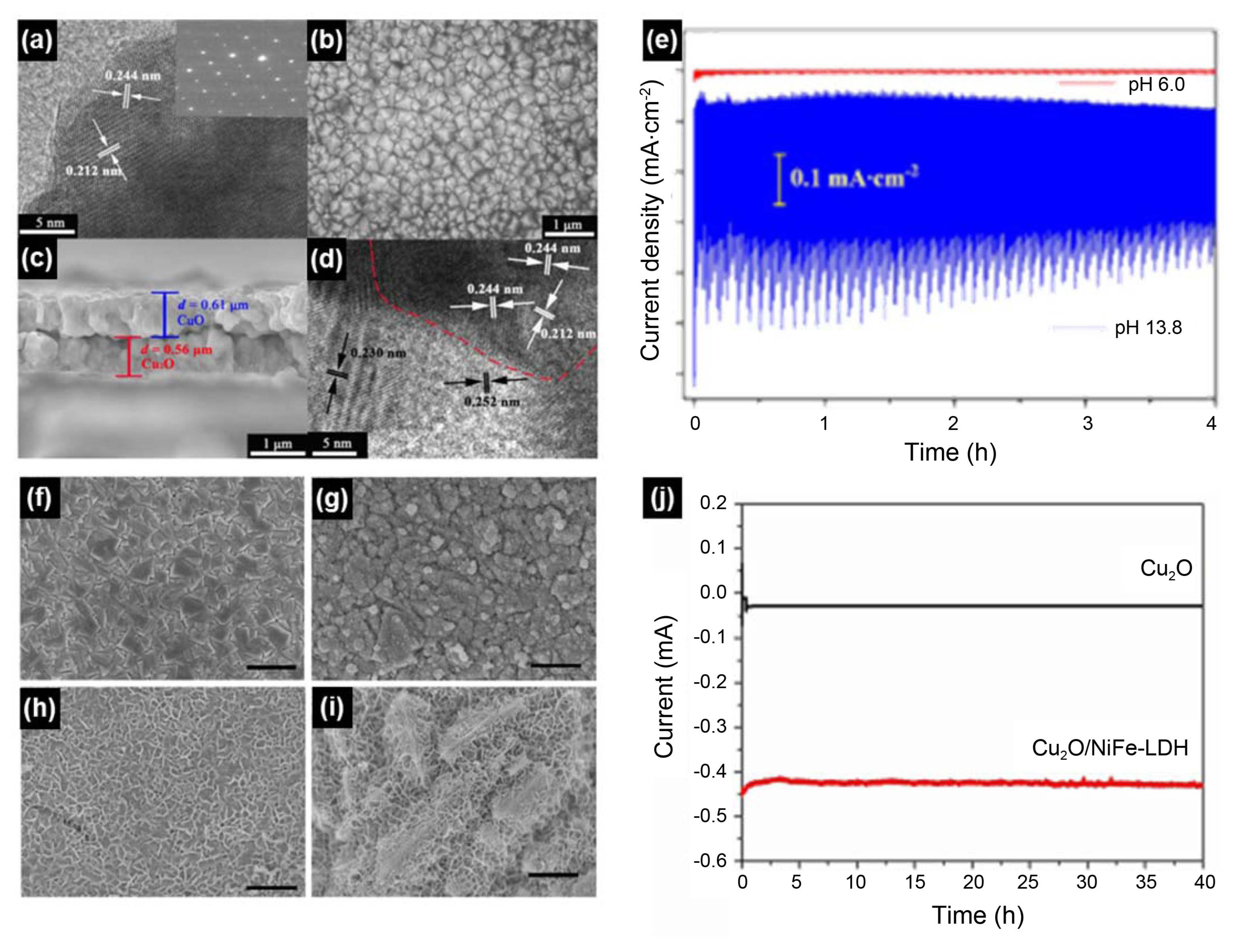
Yang et al.95) demonstrated a Cu2O/CuO bilayer composite synthesized by a facile method that involved electrodeposition and a subsequent thermal oxidation, as shown in Fig. 11(a)-(d). This strategy of combining electrodeposition and thermal oxidation provides an easy, low cost, and scalable strategy to prepare Cu2O/CuO heterogeneous photocathodes for HER. The Cu2O/CuO photocathode exhibited significantly high photoactivity and good photostability toward HER, especially at high potentials in alkaline solution. The photocurrent density for HER was 3.15 mA/cm2 at a potential of 0.40 V vs. RHE, which was one of the highest reported values at the same potential on copper-oxide-based photocathodes. Good photostability was seen during the 4 h measurements.
Qi et al.94) introduced NiFe-layered double hydroxide (NiFe-LDHs) overlayers as co-catalyst on Cu2O electrodes via electrodeposition and studied their PEC behavior, as shown in Fig. 11(f)-(j). The electrodeposition enabled the synthesis of uniformly-anchored NiFe-LDH layered nanoplates onto the Cu2O surface. The resulting Cu2O/NiFe-LDH exhibited a remarkable 7-fold enhancement of photocurrent density under an applied voltage as low as − 0.2 V vs. Ag/AgCl. Also, long-term photostability tests revealed that Cu2O/NiFe-LDH photocathodes showed no photocurrent loss after 40 h of operation under light at − 0.2 V vs Ag/AgCl low bias condition, which makes Cu2O/NiFe-LDH photocathode a good candidate for low bias PEC water splitting.
CuO is another well-known photocathode with an indirect band gap of 1.2 - 1.8 eV. Due to its smaller band gap, it is possible to achieve a higher photocurrent than with Cu2O, but CuO has received less attention than Cu2O for use as a photocathode in solar water splitting. This lack of attention is probably because of uncertainty as to whether the photo-excited electrons in CuO could reduce water to H2 (the conduction band minimum of CuO is reported to be between 0 and − 0.2 V vs RHE, which is more positive than that of Cu2O).98) Also, photocorrosion of CuO is another limiting factor for use in PEC water splitting. Recent studies showed suppressed photocorrosion of CuO.98-99)
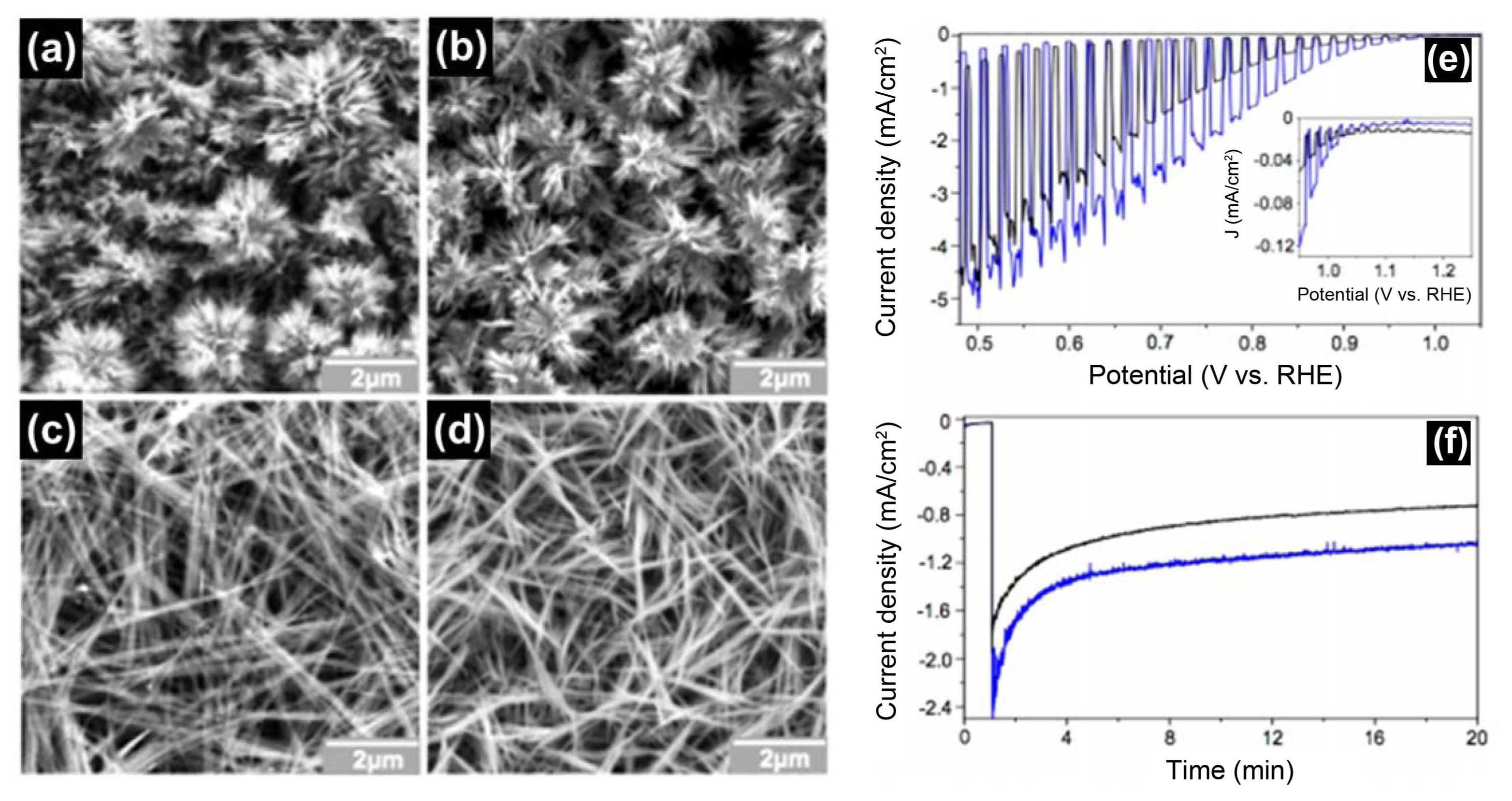
Cardiel et al.100) developed novel electrochemical synthesis methods to produce copper hydroxyl double salt (Cu-HDS) films with four different intercalated anions (NO3−, SO42−, Cl−, and dodecyl sulfate) as pure crystalline films, deposited as (Cu2NO3(OH)3, Cu4SO4(OH)6, Cu2Cl(OH)3, and Cu2DS(OH)3), as shown in Fig. 12. These methods are based on p-benzoquinone reduction, which increases the local pH at the working electrode and triggers the precipitation of Cu2+ and appropriate anions as Cu-HDS films on the working electrode. The resulting Cu-HDS films could be converted to crystalline Cu(OH)2 and CuO films by immersing them in basic solutions. The CuO films prepared from Cu-HDS films have unique low-dimensional nanostructures, creating high surface areas that cannot be obtained by direct deposition of CuO, which has a 3D atomic-level crystal structure, since Cu-HDS films were composed of 2D crystals as a result of the atomic-level layered structure of HDS. The CuO films recorded great onset potential (> 1.0 V vs RHE) very close to their flat band potential (~ 1.2 V vs RHE), which shows great promise for use as photocathodes in PEC cells for solar water splitting.
2.2.2. Other Metal Oxides as Photocathode
To date, metal oxides as photocathodes have been focused primarily on Cu-based oxides such as Cu2O, CuO, CuFeO2 and CuBi2O4.28,101-102) However, the presence of copper in most p-type oxides is known to be a cause for photocorrosion, therefore these materials need a protection layer. Recent studies have searched for a breakthrough to solve the limitations of Cu-based metal oxides as photocathodes.
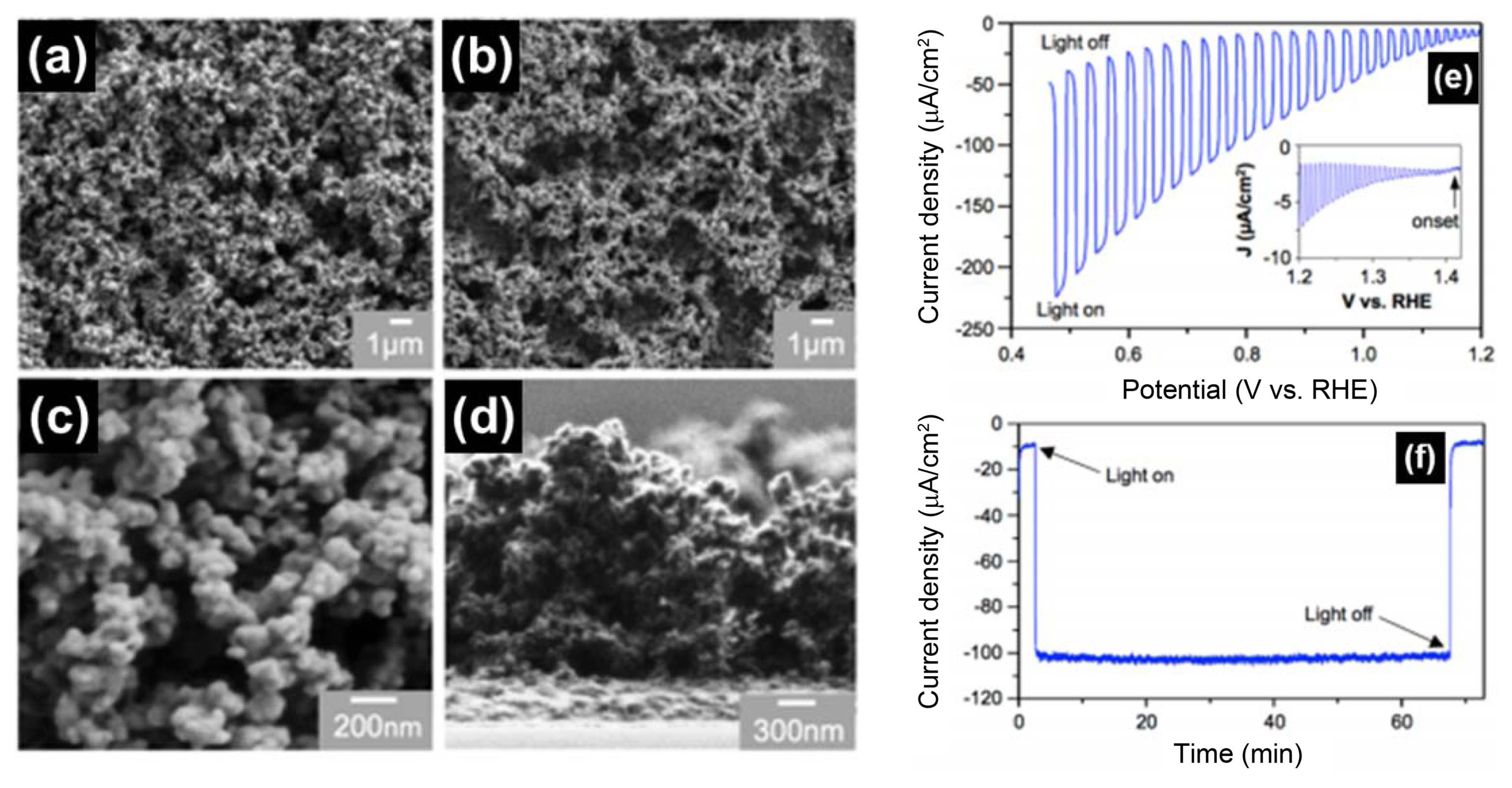
Perovskite-type lanthanum iron oxide (LaFeO3) is a p-type oxide that has several attractive characteristics such as an ideal band gap of 2.1 eV and band edger positions for use in PEC water splitting. Wheeler et al.103) reported nanoporous LaFeO3 prepared by electrochemical co-deposition of La(OH)3 and Fe(OH)2 via nitrate reduction, as shown in Fig. 13. The significant finding of this study is that, after 1 h of PEC measurement for water reduction at 0.5 V vs. RHE, there is a negligible portion of surface electrons being used for water reduction, and no sign of photocorrosion unlike Cu-based metal oxides. This confirmed that LaFeO3 is a rare p-type oxide that does not suffer from photocorrosion. Therefore, the enhancement of the PEC performance of LaFeO3 can be expected with systematic doping studies and by combining it with a proper hydrogen catalyst.
3. Perspective and Outlook
Based on the previous discussion, we have reported the most recent progress of solution-based metal oxides for PEC water splitting. Even though metal oxide materials have substantial potential as photoelectrodes, there remain a number of challenges that need to be overcome. Poor electrical conductivity, limited light absorption, and photocorrosion are still the main drawbacks of most metal oxides when used as photoelectrodes for PEC water splitting. Thus, various strategies have been introduced to solve these limitations and improve the PEC performance of metal oxides. These strategies include the formation of nanostructures, band structure modification, introduction of plasmonic nanoparticles, the formation of heterostructures, and co-catalyst modification, in order to increase light absorption and enhance charge transfer. The following are some suggestions for future research directions along with their challenges, to improve PEC water splitting and possibly lead to breakthroughs.
The formation of nanostructures such as nanoparticles, nanotubes, nanorods, nanocorals, and nanotrees is a promising approach to enhance photoactivity. Morphology control provides an effective pathway for charge transport and to significantly suppress electron-hole recombination. Most of all, 3-dimensional (3D) net structures can not only provide more active sites for solar water splitting, but also facilitate charge transport and collection. The suggested solution processes have great potential to synthesize uniform 3D nanostructures and enable conformal deposition on various 1D nanostructures. The formation of type II heterojunctions has been recognized as an attractive route to promote efficient charge separation, which enlarges the interfacial area and improves optical absorption, thus it is crucial to find the best junction materials. Modification of band structure is a powerful approach to modify electronic structure and surface structure. The proper configuration and distribution of foreign dopants in semiconductor materials can optimize their electronic structures for efficient harvesting of sunlight.104,105) Co-catalysts have played a critical role in the solar water splitting reaction,106) such as reducing charge recombination, increasing reaction kinetics, and protecting materials from chemical corrosion, thus it is necessary to develop co-catalysts with cost-effective and superior properties. Plasmonic nanoparticles can increase the photocurrent density of metal oxides to exceed theoretical values, since three critical enhancement factors of plasmonics: hot electron injection, plasmonic resonance energy transfer, and scattering, can simultaneously operate. A further research field in PEC water splitting is to develop a suitable technology for large scale photoelectrode fabrication and cost-effective solar fuel production to compete with fossil fuel. All of the above strategies for developing efficient solar water splitting system can be satisfied by solution processes. Solution processes such as hydrothermal and electrodeposition facilitate the synthesis of uniform and 3D nanostructures by controlling parameters and enabling large-scale synthesis without restriction of electrode size. When considered together, it is clear that solution-based methods are a very promising pathway for cost-effective PEC cell fabrication systems.
In this article, we have reviewed recent progress in the field of nanostructured metal oxides synthesized by solution processes for PEC water splitting. We divided metal oxides into photoanodes and photocathodes. Unlike many impressive results that have been achieved in the use of metal oxides as photoanodes, research on metal oxides as photocathodes is markedly insufficient. In the future, it is necessary to find good candidates for photocathodes to make overall progress in PEC water splitting systems. Thus we believe that, besides improving the performance of existing metal oxide semiconductors, searching new metal oxide materials with highly efficient photocatalytic activity is also of crucial importance for PEC water splitting.