


1. Introduction
Plasma dry etching process used mainly for micro patterning in semiconductor processes based on Silicon or aluminum are known to have high etching selectivity due to anisotropic etching.1) Owing to this process, micro-patterning was made possible, enabling miniaturization of all electromagnetic devices currently used by us.2-4) Meanwhile, in the recent times where the width of micro patterns has been reduced to the level of 10 nm, removal of contaminants such as particles produced during semiconductor processes became important. In particular, polycrystalline sintered alumina mainly with coating of Y2O3 having good plasma resistant characteristics has been used as an inside lining material for the semiconductor equipment where plasma etching is implemented.5-9) Surface damages as well as fluoridation are produced in the lining material as a result of repeated plasma etching over a long time. Surface damages and fluoride products are known to induce direct problems where nano- to micron-size particles are dropped off of the ceramic lining material during long-time process, contaminating wafers.10)
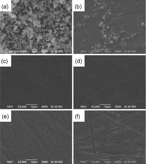
Since the production costs are excessively increased if the ceramic lining material is consumed as a disposable material, the parts employed for semiconductor processing equipment are being recycled after cleaning. For cleaning of the contaminated ceramic lining materials, acids such as nitric acid or sulfuric acid have been used to this process.11,12) As shown in Fig. 1, since alumina with the surface cleaned by acids has roughened surfaces accompanied by exposure of internal pores, considerable amounts of time are required upon application of the recycled item as a result of the acid treated Al2O3 inducing problems such as particle contamination in semiconductor processes. Namely, in application of the recycled ceramic lining material to processes, there is an initial particle problem which is different from plasma corrosion and occurrence of contaminating particles produced upon long-term use. When a new ceramic lining material is mounted in semiconductor and display processes, similar problems are also known to occur although the time is short. To suppress such initial particles and outgassing, plasma resistant characteristics have been evaluated for the glass materials having diversified characteristics per composition.
Lee et al have attempted development of materials which not only have permeability but also excellent plasma resistant characteristics by using glasses containing rare earth elements as a material to substitute for quartz or sapphire employed for the window glass in plasma equipment.13) Although plasma resistant characteristics were affirmed for the rare earth-containing glasses, there existed problems of having disadvantages such as expensive raw material prices of rare earth and high manufacturing temperature of 1700°C required.
In the present study, plasma resistant characteristics for CF4 /O2 /Ar mixture plasma have been evaluated for the object of several glasses which are already known to be resistant to hydrofluoric acid or chemicals. Also, plasma resistant characteristics have been comparatively evaluated by selecting zinc aluminum phosphate glass based on consideration of plasma resistant characteristics and thermal expansion coefficient, alkali-free aluminosilicate glass, boric acid glass having chemical stability and Y2O3-containing yttrium aluminosilicate system known to have high plasma resistant characteristics as the glass material to be coated onto the damaged alumina surface.14-16)
2. Experimental Procedure
Compositions of the glasses as the object of the present experiment are summarized in Table 1. As the raw materials for the glass prepared by melting method, SiO2, Al(OH)3, ZnO, P2O5 (99%, DAEJUNG, Korea) and Y2O3 (99.9%, KOJUNDO, Japan) were selected, and commercial borosilicate and glass composition based on calcium aluminosilicate being applied to LCD panel were used for the compositions of BS and CAS, respectively. The samples of 50 g each per composition were mixed by using a 3-dimensional mixer at 50 rpm for 3 h to homogenize the composition. Subsequently, heat treatment was conducted in a Rh-Pt crucible at a heating rate of 10°C/min for holding at 1600°C for 2 h using an electric furnace of oxidizing atmosphere. After undergoing melting process, the molten body was cooled by air cooling method for vitrification at room temperature. Thermal stress produced in the glass during cooling process for vitrification was relieved through annealing for 2 h at a temperature higher by 50°C than the glass transition temperature measured per specimen. To determine vitrification status, X-ray diffractometer (DMAX-2500, Rigaku, Japan) was employed.
Thus-produced glass specimens were made into the size of 10 × 10 × 1 mm3 in length x width x height for plasma etching test, and mirror polished to have the surface roughness (Ra) of less than 0.05 μm for uniform etching. The prepared specimens were then placed on a 6-inch Si wafer and subjected to masking processing with Kapton tape on them. For masking processing, 3 layers were overlapped on the tape at an interval between tapes of about 1 mm. To compare plasma resistant characteristics as a function of glass compositions with that for the material used in the past, alumina was employed. Plasma etching experiments were conducted by using a polymer etcher(TCP-9400DFM, Lam Research, USA) in the clean room. Detailed plasma etching conditions are shown in Table 2.
To evaluate plasma resistant characteristics, etching rates were measured for the object of specimens with plasma etching reaction implemented. Here, a mean step for etching rates was obtained by repeated measurements for 5 times by using Alpha Step (Surfcorder ET 3000, Kosaka Lab, Japan), followed by comparative analysis of etch rates per specimen by using an error bar chart for mean values and deviations. In addition, not only etching rates but also surface roughness after reaction to plasma etching was shown by the same equipment. Also, to check for surface state of the etched parts and reaction products between plasma and for glass composition components or contaminants such as particles, microstructures were observed by using scanning electron microscopy (JEOL, JSM-6701F, Japan). For the composition analysis of commercial glass compositions, ICP-OES (OPTIMA 5300 DV, PERKIN-ELMER, USA) and XRF (ZSX Primus, RIGAKU, Japan) were employed.
3. Results and Discussion
In Fig. 2, a schematic diagram for plasma reaction and etching process occurring in the material is summarized.17) In the etching with the use of plasma, particles ionized by granting electrical energy in the state of neutral gas are used. And, by granting electrical energy to CF4, O2 and Ar neutral gas, the ionization processes can be shown approximately by the equations (1), (2) and (3), respectively.18)
Through the ionization to neutral gas, fluorine radicals and Ar+ ions are mainly formed through the above reactions. In plasma etching process, physical ion collisions within the sheath potential through sputtering of Ar+ ions and chemical reaction between fluorine radical and the etched material take place on the surface. After generation of reaction products due to reaction between material surface and plasma through this process, desorption reaction from the substrate occurs.19,20)
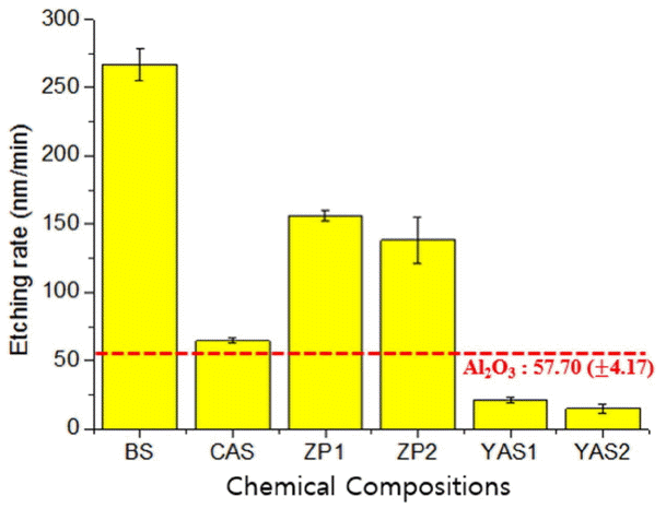
Etch rates for the compositions of borosilicate (BS) and calcium aluminosilicate (CAS), the glass compositions of zinc aluminum phosphate (ZAP) system and yttrium aluminosilicate (YAS), along with polycrystalline alumina currently used for a plasma resistant material as the reference materials for comparison with these are shown in Fig. 3. Etch rates of the glasses having BS, ZAP1, and ZAP2 compositions were 268 nm/min, 164 nm/min, and 145 nm/min, respectively, being relatively higher than the etch rate for polycrystalline alumina of 57 nm/min. On the other hand, etch rates of the glasses having CAS, YAS1, and YAS2 compositions were 64 nm/min, 23 nm/min, and 14 nm/min, respectively, showing similar or lower etch rates compared with that for polycrystalline alumina. Namely, with alumina as reference, etch rates for CAS and YAS-based compositions were measured to be similar or lower, whereas those for BS and ZAP-based compositions were measured to be relatively much higher. As a reaction product due to chemical reaction between glass composition on the surface and fluorine radical during plasma etching process, fluoride compounds were formed. Considering Table 3 for summary of sublimation points for fluorides per element, all sublimation point points for boron, silica, and phosphate as the major components for BS and ZAP-based compositions were lower than −80°C, having volatilization characteristics due to fluoride reaction, whereas all sublimation points for the fluorides of yttrium, calcium, and aluminum among the compositions included in CAS and YAS had values higher than 1,200°C.21,22) The cause for showing different etch rates per composition is attributed to the sublimation temperature as fluoride compounds were formed within the glass compositions due to chemical reaction in the plasma etching process.
Although ZAP-based composition was expected to have excellent plasma resistant characteristics as it was known to have high resistance to hydrofluoric acid, a higher etch rate than that for alumina was measured. Etching by not only fluorine radical but also ionized Ar+ makes contribution to plasma etching. Hence, resistance to physical etching by Ar+ as well as chemical reaction due to fluorine should be considered for plasma resistant materials. Shin et al considered the relationships between glass transition temperature (Tg) and weak interatomic binding force,23) while Ojovan stated that Tg was a temperature range in which stable arrangement of atoms was realized as interatomic inter-diffusion took place in the relevant temperature range and that interatomic bonding was strong if the transition temperature was high.24) The cause for the high etch rate with ZAP is considered attributable to not only volatile characteristics of PF3 compound as the major component for phosphate but also low interatomic bonding energy.
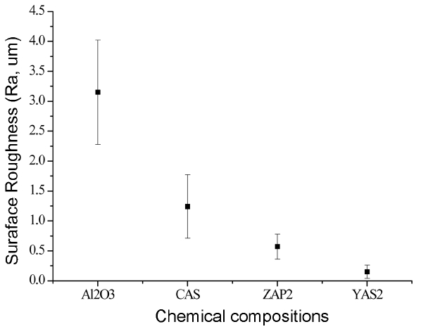
According to the article published by Kim on plasma resistant characteristics as a function of plasma etching variables for SiC material, etch rates showed a relationship of being proportional to surface roughness and DC bias.25) Fig. 4 shows surface roughness values for the surfaces of alumina and representative specimens per composition after plasma etching. For CAS, the value of 1.24 μm was measured despite a relatively low etch rate compared with other glass compositions, which represents the highest surface roughness value among all glass compositions. While the rather low surface roughness of 0.57 μm was measured for ZAP2 in comparison with CAS, it showed a high surface roughness when compared with that for YAS-based glass composition. And, the value for YAS2 of 0.15 μm showed not only the lowest etch rate, but also allowed affirmation of the smoothest surface of all glass compositions.
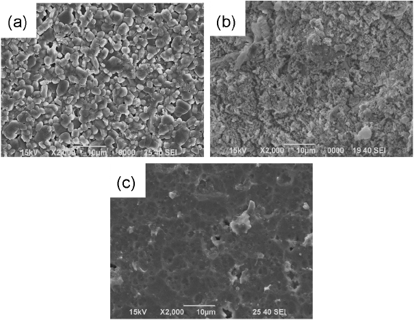
Figure 5 shows microstructures observed to check for the causes for different surface roughness values per composition, surface state and reaction products after etching, and contaminants in the form such as particles observed in alumina. In CAS composition, the reaction products of 0.5 ~ 3 μm in size were observed, due to which the highest surface roughness is considered to have been measured among the glass compositions. Although BS was expected to show a high etch rate along with a surface microstructure with clear occurrence of etching having no reaction products due to low surface roughness, reaction products having diversified forms were observed with a nano size of less than 0.5 μm. And, in general, the etching process not only removes surface materials but also changes surface morphologies. ZAP 1 and 2 showed a morphology such as glassy surface with microstructural shape changed due to etching by hydrofluoric acid solution.26,27) This shows clear occurrence of inward etching, and is considered to represent the surface etched as phosphate composition in ZAP was volatilized due to reaction with fluorine. Lastly, although the parts expected as damage produced during fabrication process were observed in YAS1 and YAS2, no other phenomenon due to plasma etching was discovered, allowing affirmation of excellent etching resistance for the present material.
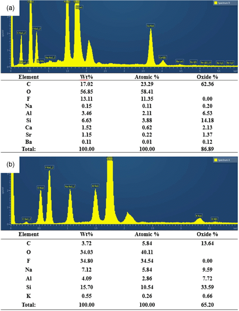
Figure 6 shows the EDS analysis results for chemical compositions of the reaction products observed in CAS and BS microstructures. For the reaction products of 0.5 ~ 3 μm in size observed from the microstructure of CAS samples, clear increase in carbon and fluorine composition which were not included in the glass can be affirmed. And, carbon and fluorine compositions were also affirmed according to the EDS analysis results for the reaction products which were more clearly observed than in BS. As more than 90 wt.% of BS consists of SiO2 and B2O3 with the balance being comprised of Na2O and Al2O3, fluoride of low sublimation can be generated. According to Aoki, boron trifluoride produced by reaction between boron element and CF4 was reported to be sublimated accompanied by occurrence of byproducts, which can be expressed by the equation (4).28) Therefore, the byproducts observed in the microstructure after corrosion test of the glasses with BS and CAS compositions are considered to remain in the fluorides such as NaF, AlF3, etc. together with the reaction products of CFx polymer type due to the reaction of equation (4).
CAS composition has a chemical composition where CaO and B2O3 were added to aluminosilicate base. 10 wt.% of B2O3 having volatilization characteristics as a function of Fluoride was added, and CaO showed an etch rate on the level similar to that of alumina although only 8% of the total was added. This may be caused by a relatively low SiO2 content and a high Al2O3 content. In the future, plasma resistant characteristics for fluorine plasma need to be evaluated for the object of glasses with CaO being mixed as the main composition.
Glass is a mixture made of mixing diversified compositions having different properties each elements. Interior of YAS has oxygen bridges formed through ionic bonding and covalent boding of SiO2, Al2O3 and Y2O3 as the glass former and the intermediate. Whereas the glass surface is volatilized due to a low sublimation point in the case of SiO2 as a result of chemical reaction with fluorine radical in plasma etching process, Y2O3 and Al2O3 having sublimation points higher than 1,200°C are expected to exist in the surface in the state of fluoride compounds such as AlOF and AlF3 which were not volatilized by reaction. Simple reaction equations for the above reaction can be expressed by (5) and (6).
Since the reactions on the glass surface between glass composition and plasma are more complicated than the reaction equations (5) and (6), accurate reactions of the formed products such as fluoride compounds after surface reaction need to be affirmed. For this purpose, in-depth studies will be conducted in the future with application of analysis techniques such as XPS and FT-IR which would allow identification of binding energy on an atomic scale, relative ratio between elements, type of binding and accurate molecular structures such as functional group for the products after reaction.
4. Conclusions
In the present study, plasma resistant characteristics were evaluated by comparing various oxide glasses and polycrystalline sintered alumina for dry etching by mixture plasma of CF4/O2/Ar. In YAS series, the lowest etch rate of 14 nm/min and flat surface with existed scratch could be affirmed in YAS2 composition having higher yttrium content. In addition, the etch rate of 64 nm/min similar to that for alumina could also be affirmed in CAS composition. Based on this result, it can be seen that plasma resistant characteristics to fluoride plasma are increased if yttrium element is added to the glasses of an amorphous structure. On the other hand, boron, phosphate and silicon elements contained in the glass were volatile, showing high etch rates as sublimation points of all fluoride reaction products had values lower than −80°C.
In general, it was affirmed that glass composition with high resistance to hydrofluoric acid or chemicals did not exhibit excellent plasma resistant characteristics. Differences in the component elements added to glass composition were affirmed to show different plasma resistant characteristics. Namely, it could be affirmed that glasses containing the elements capable of forming fluorides having a high sublimation point with fluorine radical among glass compositions produced durability for CF4/O2/Ar plasma employed in semiconductor or display process.